
*** Newest Entries always added to the bottom ***
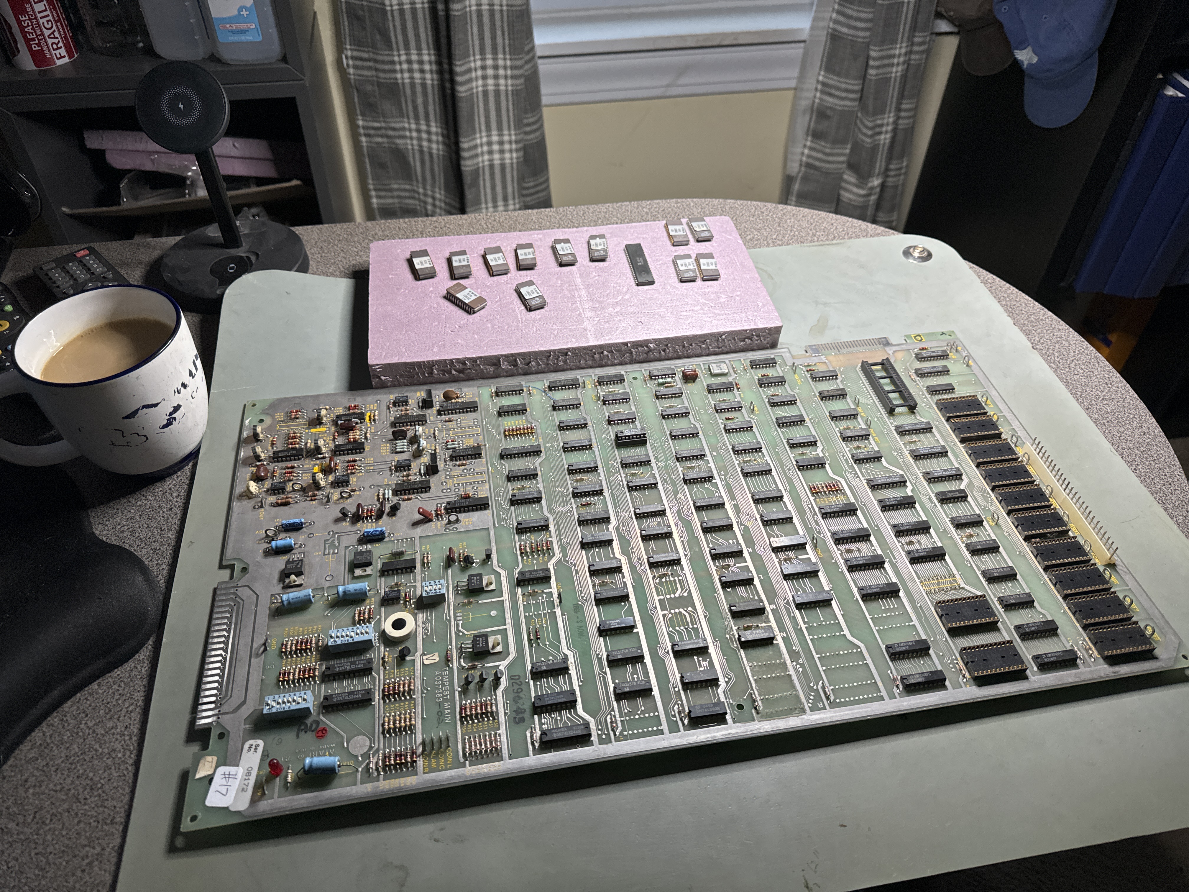
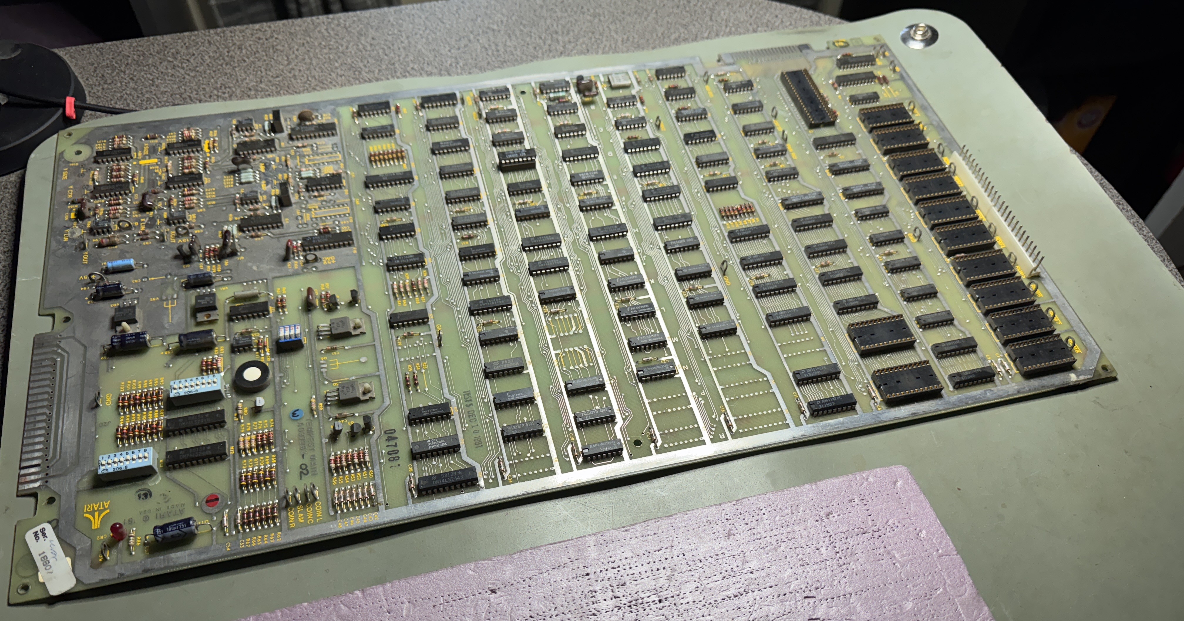
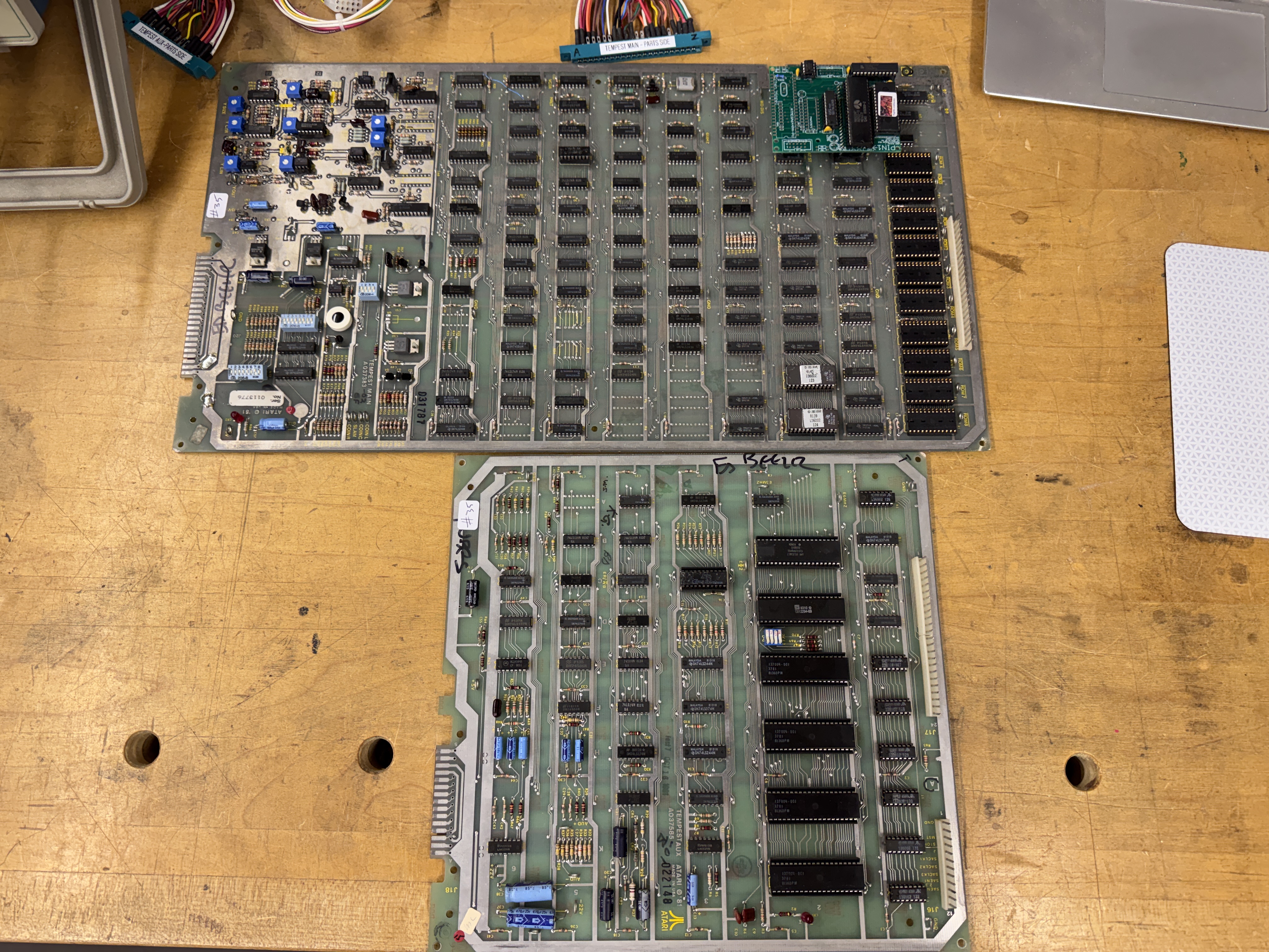
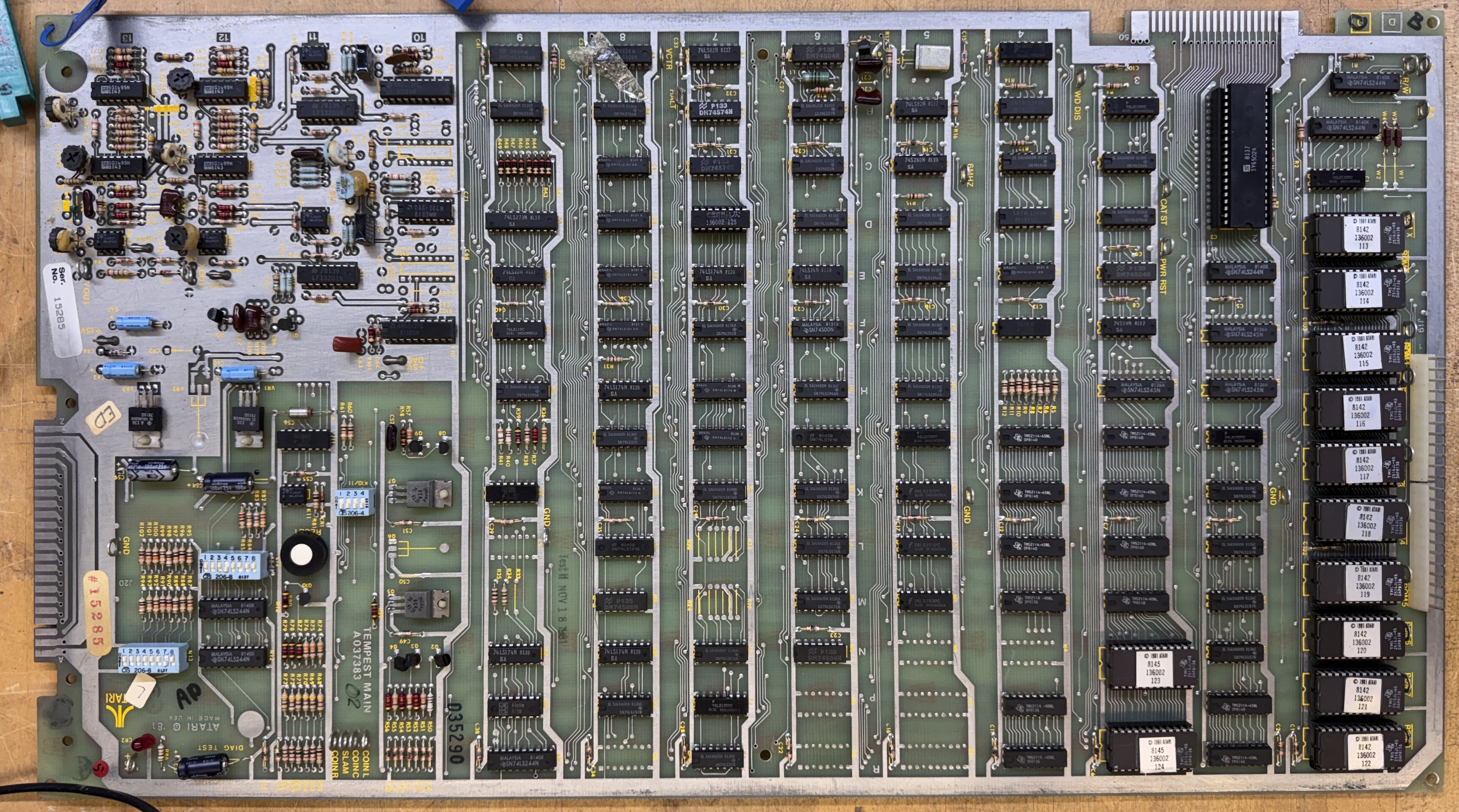
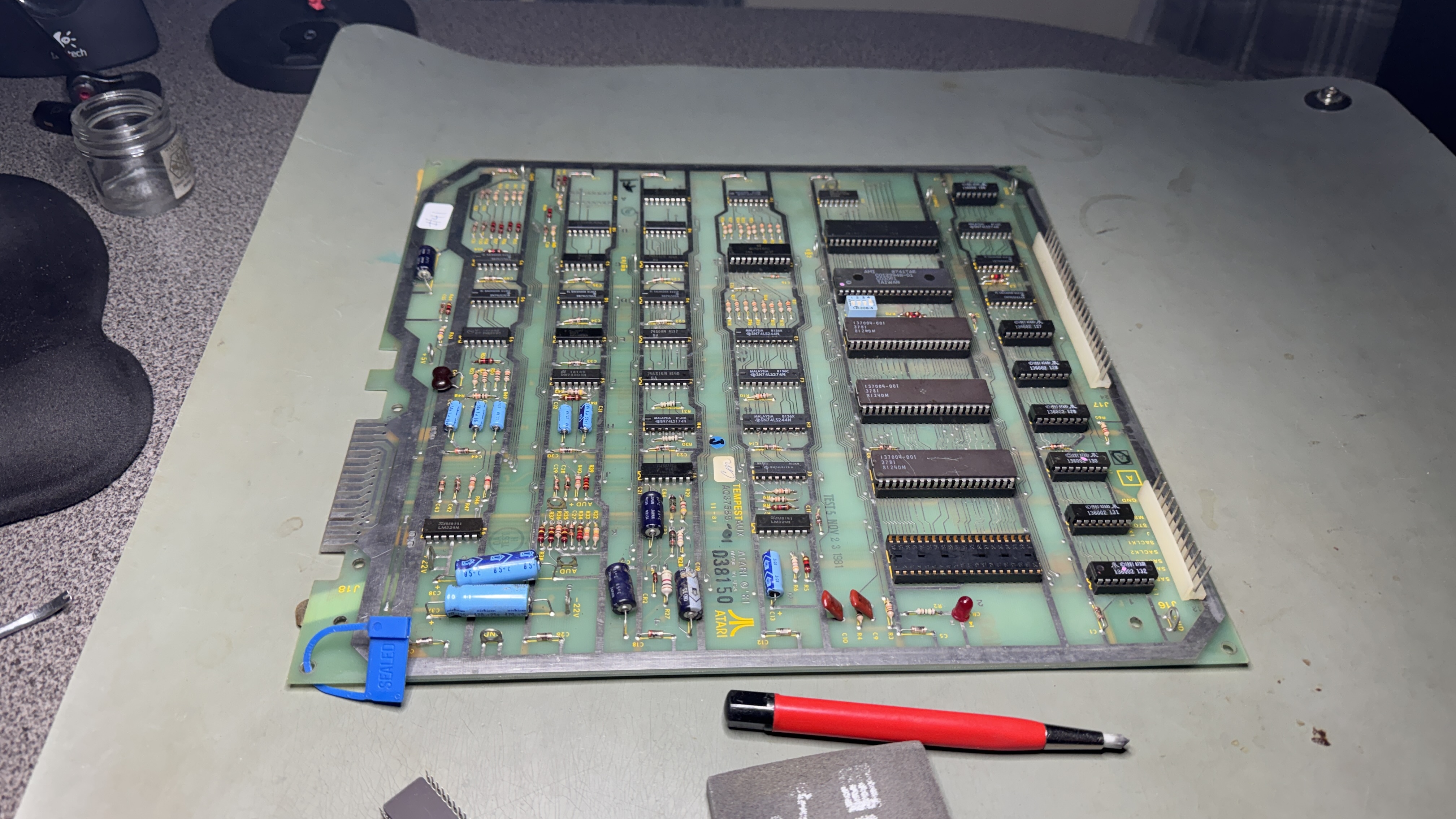
When I picked up my Tempest cabinet – I was fortunate that it came with two sets of boards. Both in unknown working condition. At some point I picked up third set to work on and later a fourth. At the top here are some of the very first PCBs I ever repaired.. My full test bench evolved as I decided repair work was something I really enjoyed.
*** Wow.. this was years ago.. Process has advanced greatly since then… ***
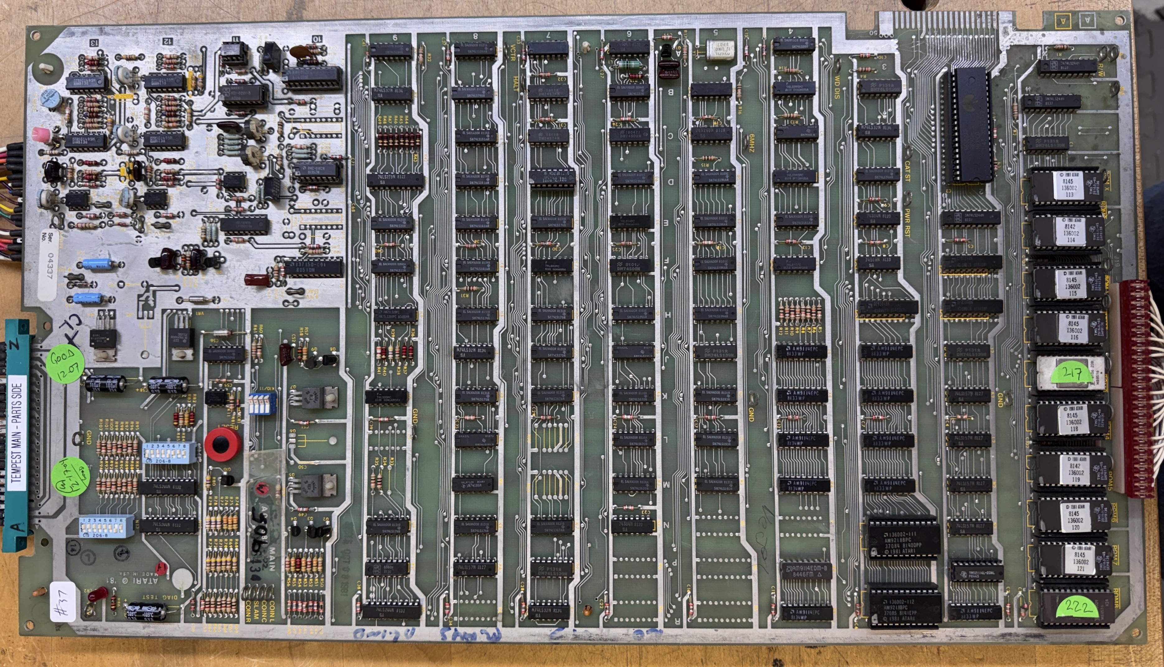
Board 1 –

My Tempest cabinet needs a fair amount of rehab work – so I removed everything to simplify the process. If I do more of these in the future – I’ll build a proper test harness. For now – The actual harness worked ok.. It’s not very good as a bench harness – not designed to allow the boards to be spread out.
Once I got things running – the board had signs of life. It was pretty flaky and it’s my first Tempest. Test mode seemed to be much more stable than game mode. In short.. pretty much anything I touched at the EPROM end of the board caused the vector engine to crash. On the scope I could see signals getting to the XY section .. but they didn’t look consistent.
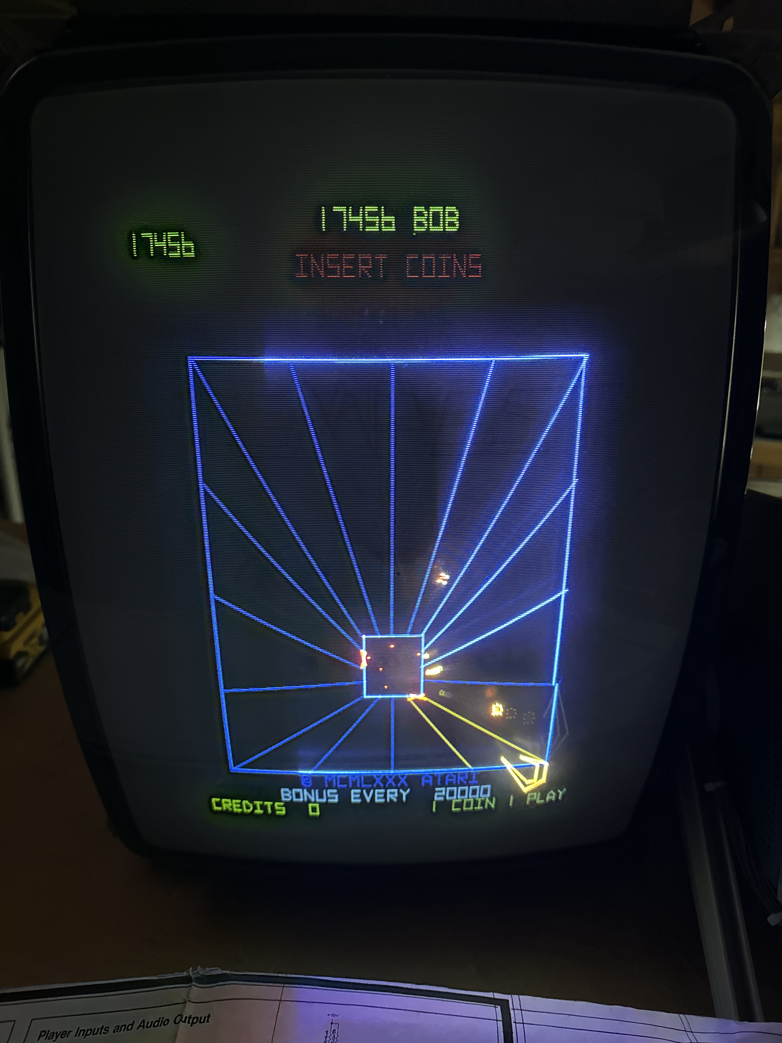
At first I thought I had issues in the analog section – however after trying a few different things. I got the game to play blind.. That’s a great start! After a few minutes it died and then complained RAM5 was bad..
Just for kicks I hit it with freeze spray, hit the reset button and the game booted again and lasted a few more minutes. Could it be that easy? (answer: no)
Pretty much every time I touched this lower corner of the board.. The game crashed. I’ve had mixed results with these original sockets. I like the gold contacts, I don’t like the design. Made the call and replaced them. Afterward – The board was a bit more stable – but I could still flex it in different areas and get it to reset. I did reflow the interconnect (it looked good and had been done before) and tested the interconnect cable.

Flexing the board while holding this guy also caused a reset. Prior work – maybe a flaky connection?
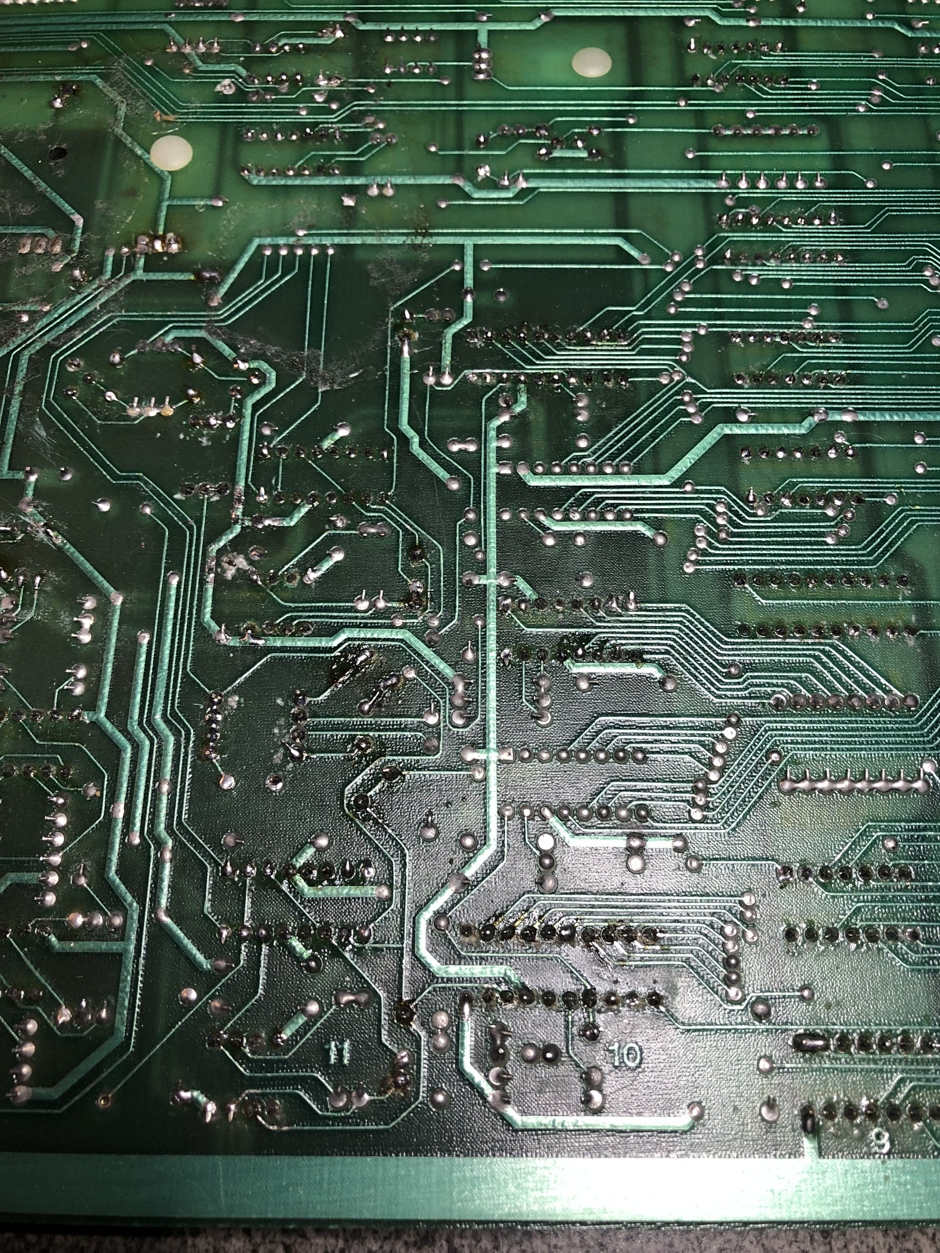
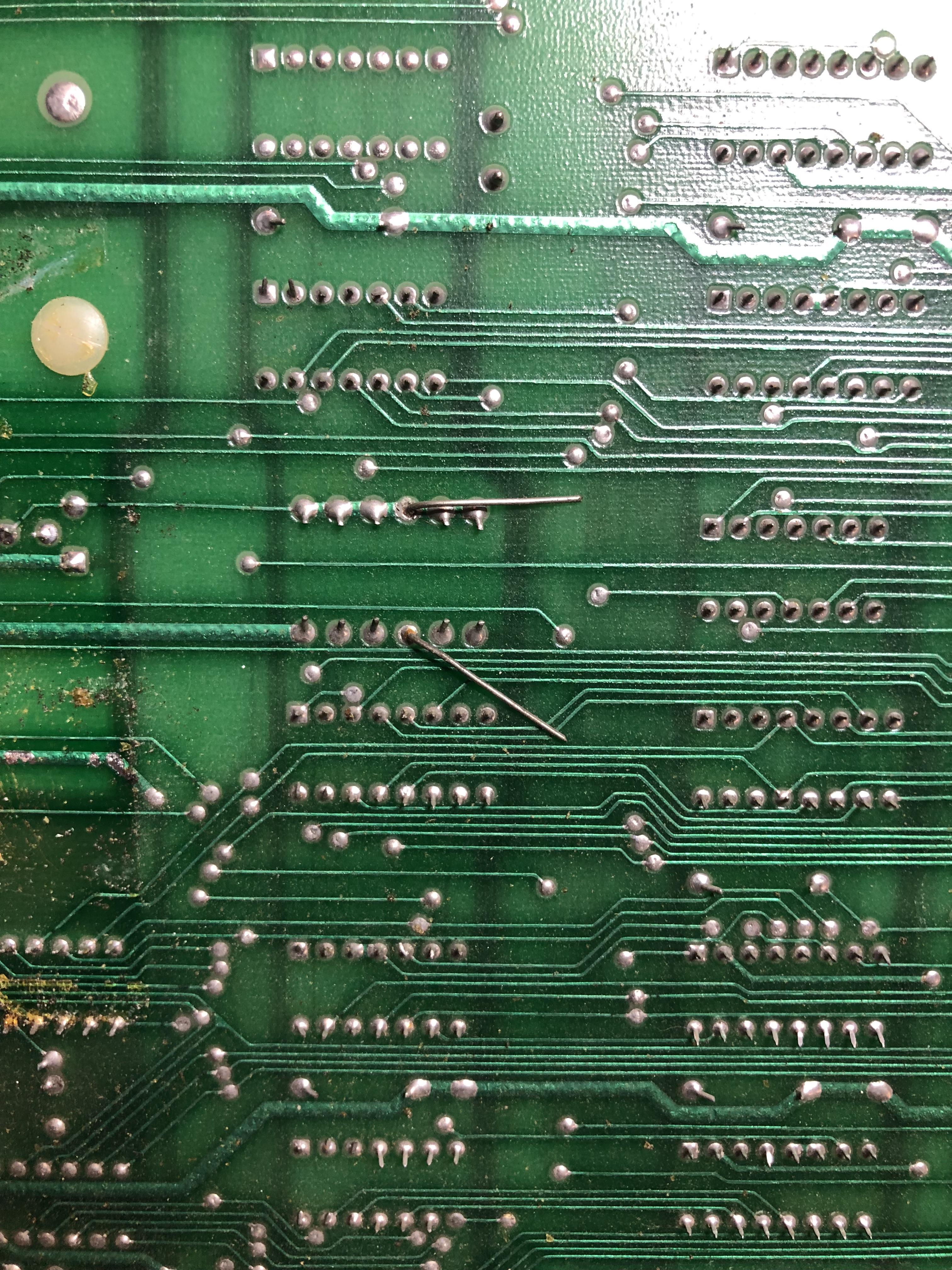
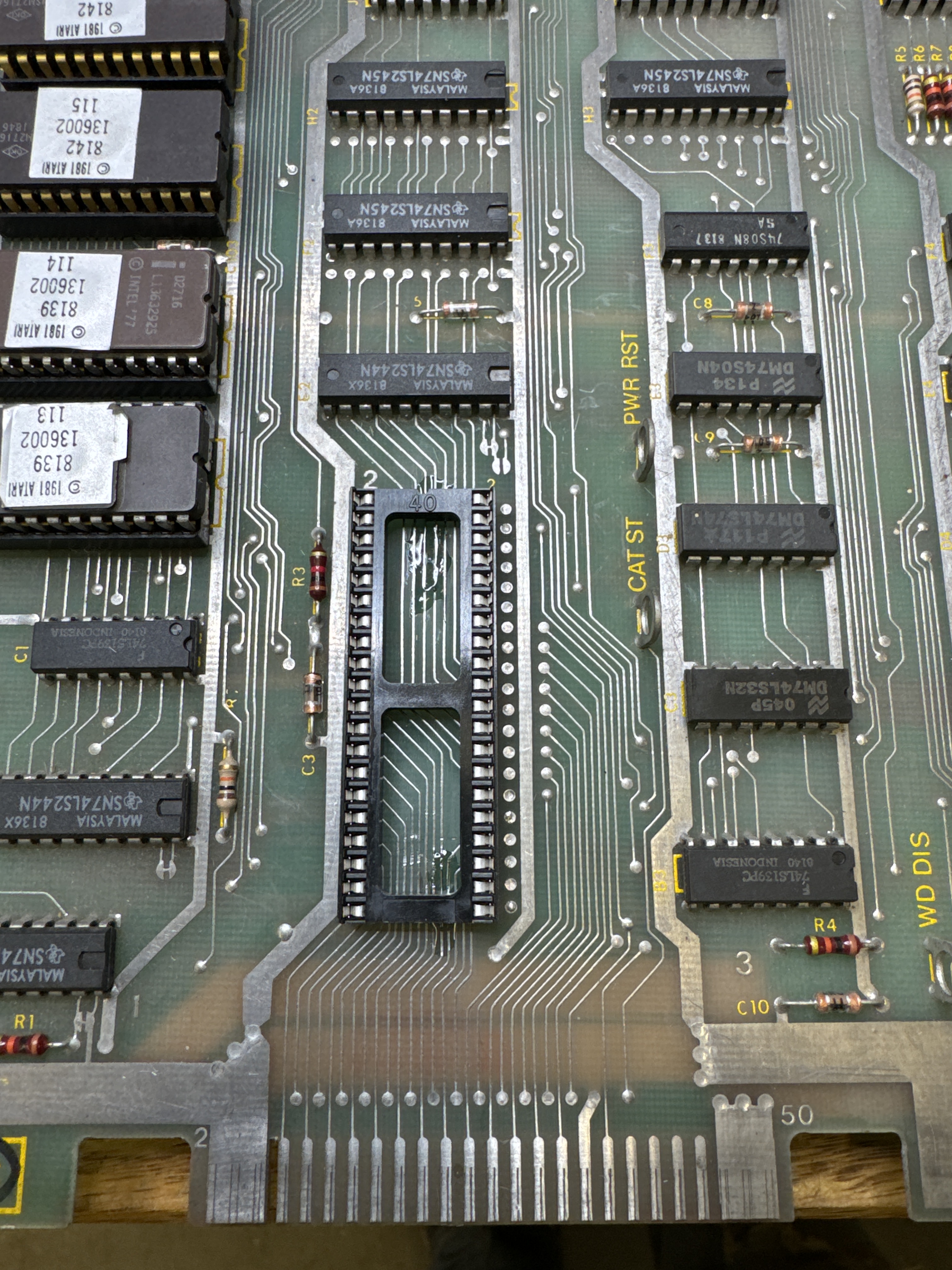
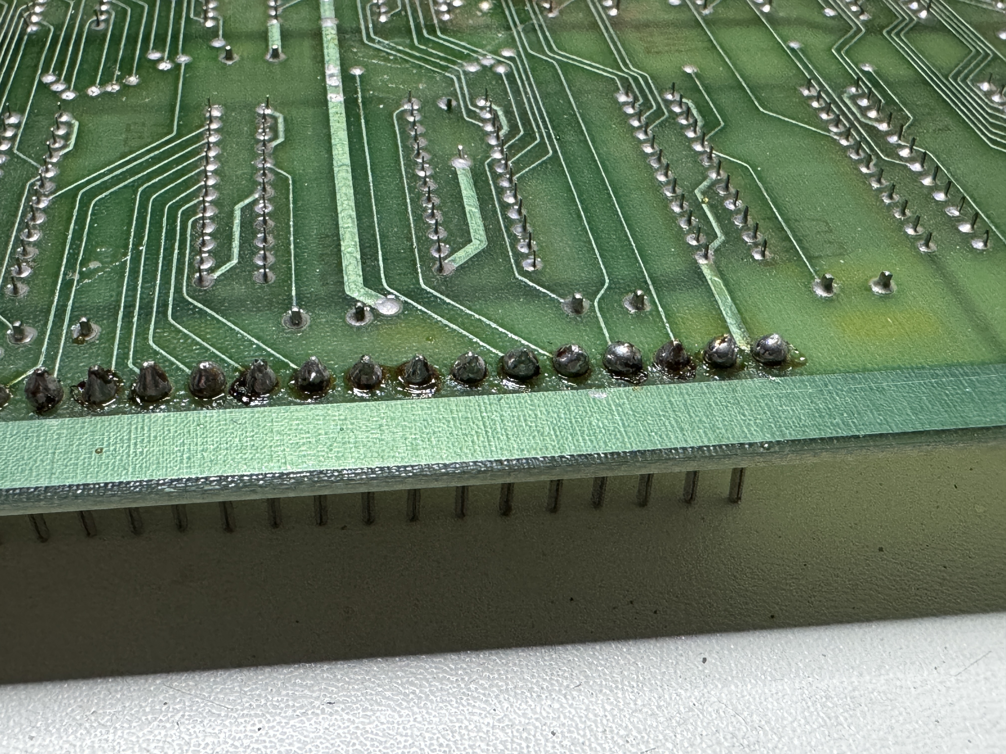
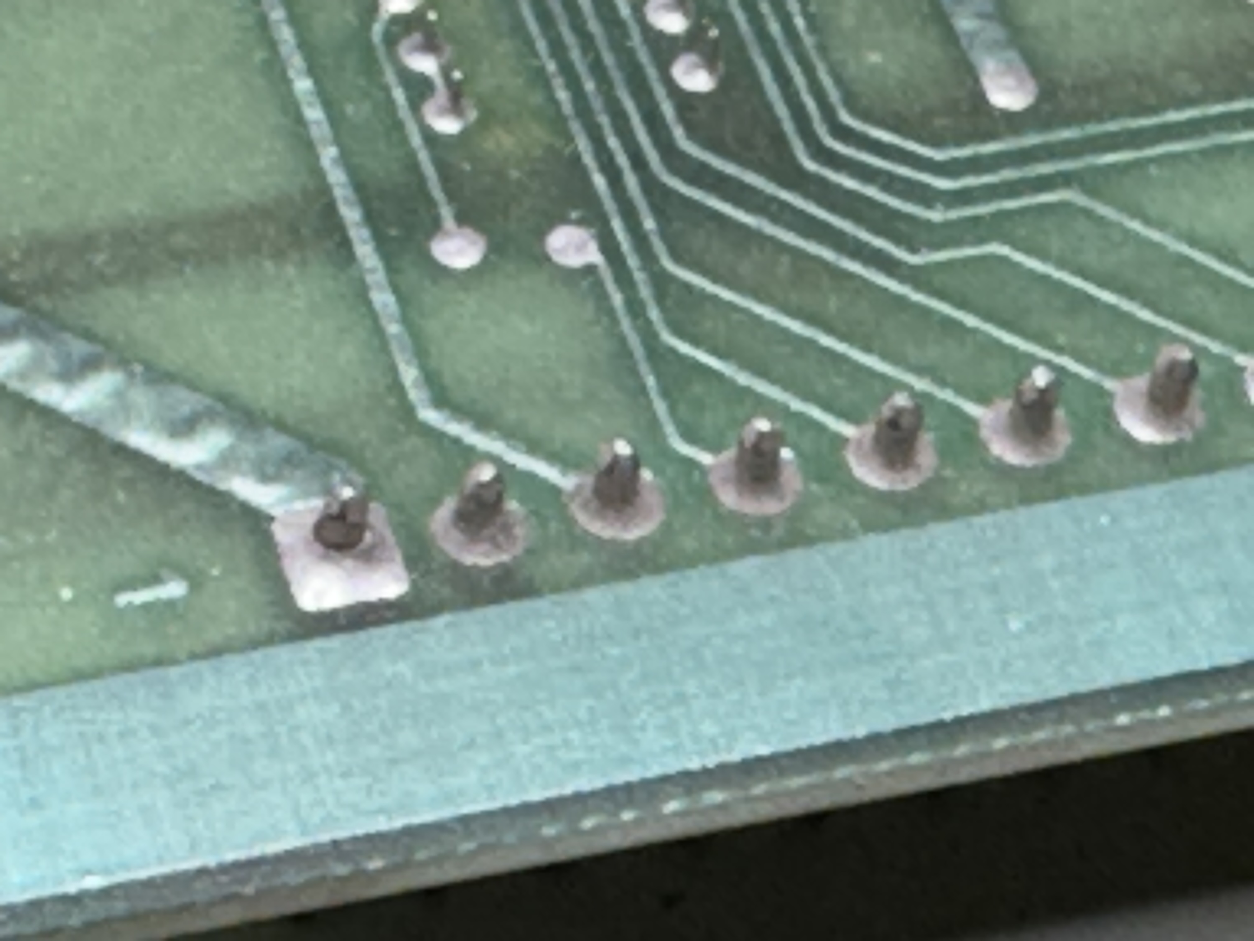
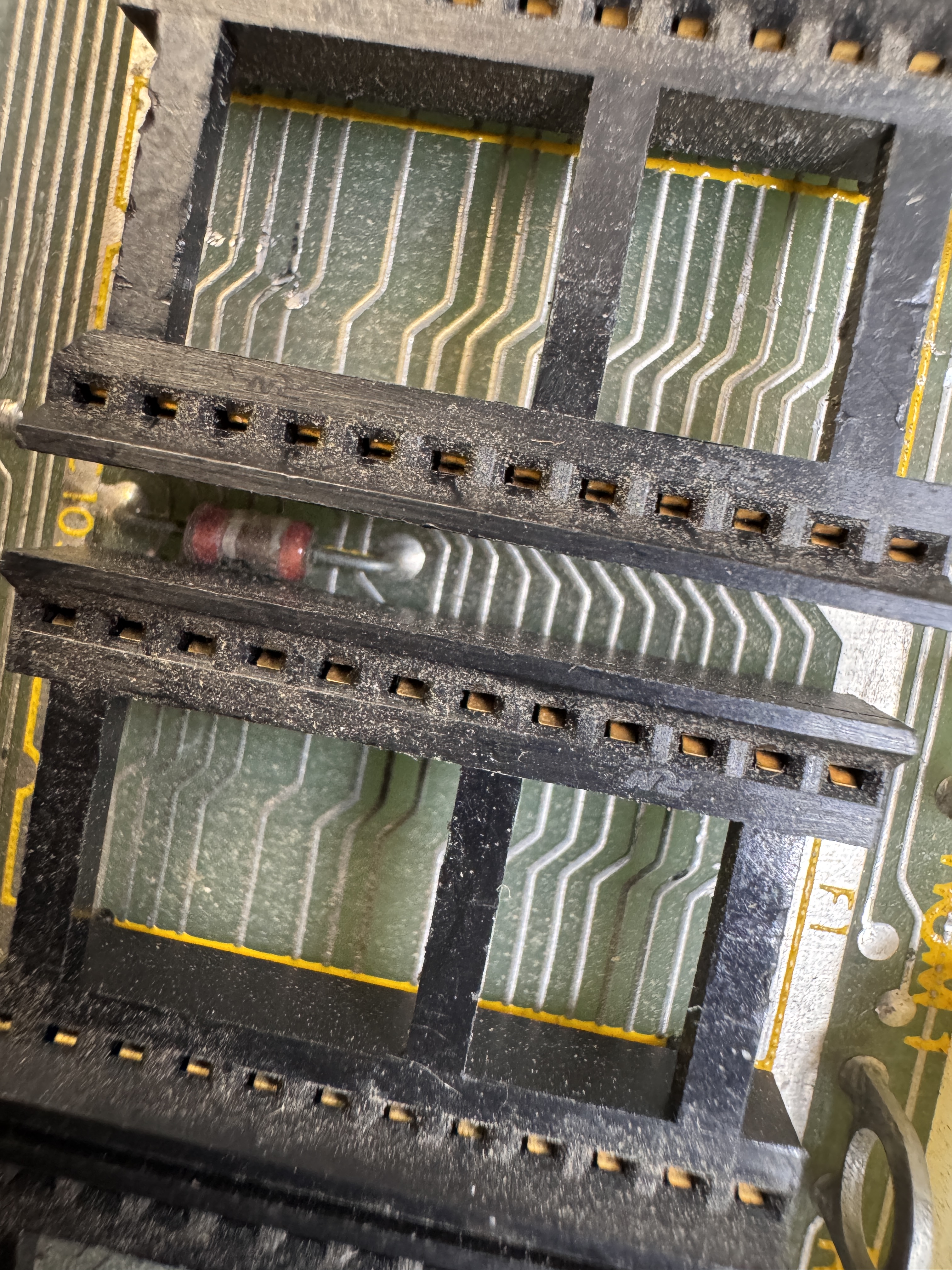
There was a lot of trace damage below the LS245. While adding Kynal wire L’s to each trace – I use a toothpick to hold everything in place.
It accomplishes three things:
– Holds wire for soldering
– Solder doesn’t stick to the toothpick
– Pushes wire to the side of the hole so I can get a socket in cleanly
The green is UV solder mask. It holds the wire in place. UV light cures it in 5-10 seconds.. Without it – the heat from soldering in the socket can cause the little wires to move. Only thing I need to do in the future is clean the flux before using the mask and get a small brush to spread it a bit neater.. (Note: I’ve since found a clear UV resin used for making jewelry that is much nicer looking and very easy to work with)

Not very pretty – but it’s not on the solder side and it’s solid Next one will be cleaner. It looks a little hackier than it is and these are really close up. Practice makes perfect. *** Note – I’ve found a clear UV cure resin since that woks much nicer and creates nearly invisible repairs ***

After all that – the board would run without crashing, unless you flexed it some more. When it crashed – it called out RAM#6. I decided to swap one in. But it was still being temperamental.
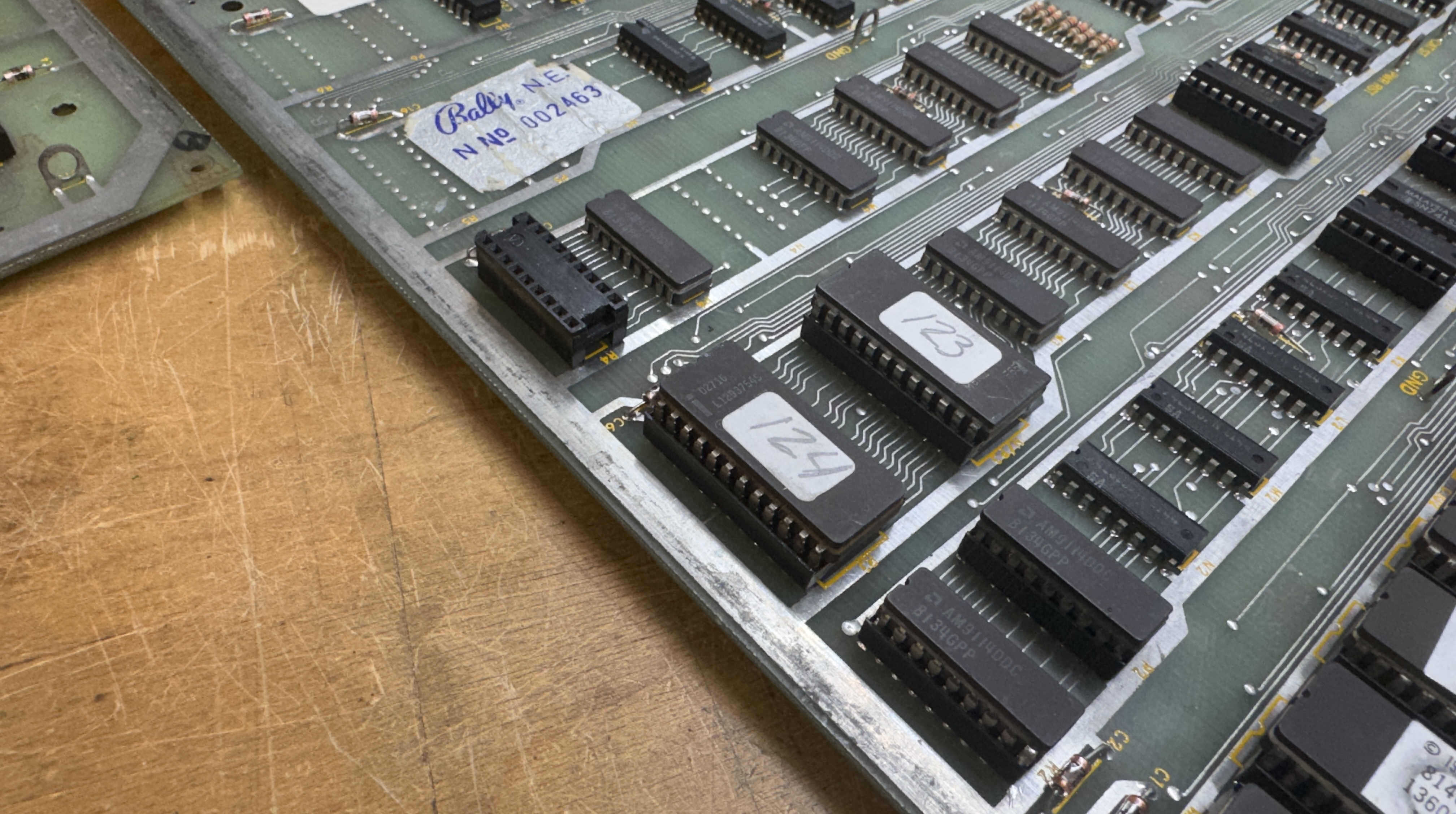
Finally after running, flexing and crashing – I was able to pinch the -111 ROM and get the machine to crash on this one chip w/o flexing. Just squeezing it in the socket. These are nice dual wipe sockets.. At the bottom of my suspect list and I had messed with it prior. Replaced the socket and I can officially beat up this board without a reset.
Both RAM I replaced were likely ok – this ROM was tripping them up.
Finally – it wasn’t retaining high scores. Swapped in a known EAROM. No changes. Tested voltage and I was only getting -14v, should be -28v. Put in new Zener diode CR2. No change. Tested CR4 and it showed open out of circuit. Replaced with a 1N4148 – High scores work again!
Board works!
Board 2 – This one I had borrowed a couple chips from..
It needs a lot of cleanup work and there is prior work..

***** I need to go back and fill in a bunch of these early repairs *****
Board 6 – Board in for repair
This one has it all.. I’m essentially taking over a repair from someone else who couldn’t get the board running.
It showed up with a lot of parts removed (and missing).. At least they were neatly removed. No board damage.
Initial Inspection:
- Missing DAC @A10
- Missing DAC @D10
- Missing TL082 @A11
- Missing Analog switch @B11 (LF13201N)
- Missing pots @R118, R119
- Half soldered MC1495 A10
- Missing C101, C107, C75, R174
- Broken Q1
- LS139 @B3 bent up
- Plenty of prior work and some trace repairs
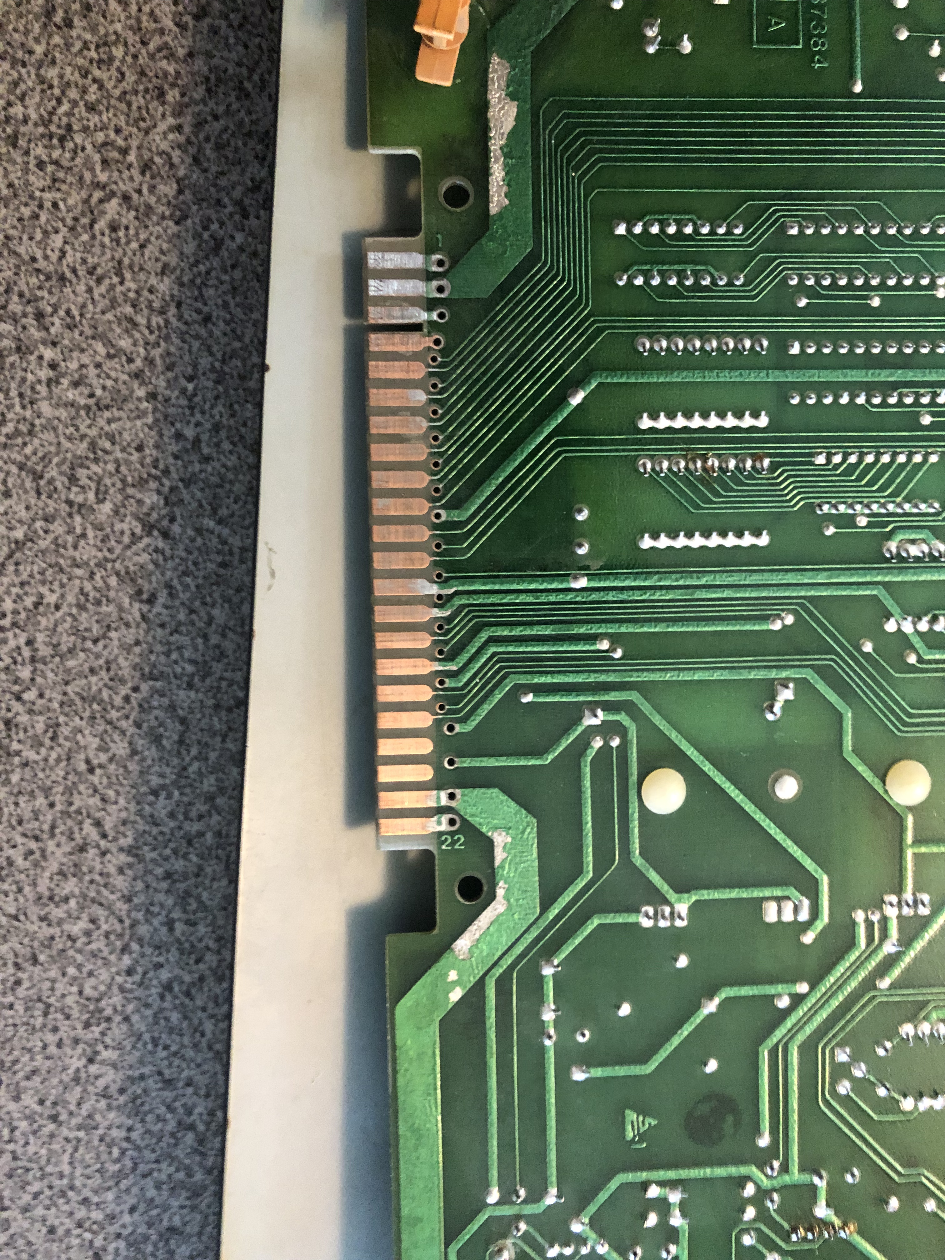
- Edge connectors needed to be reflowed
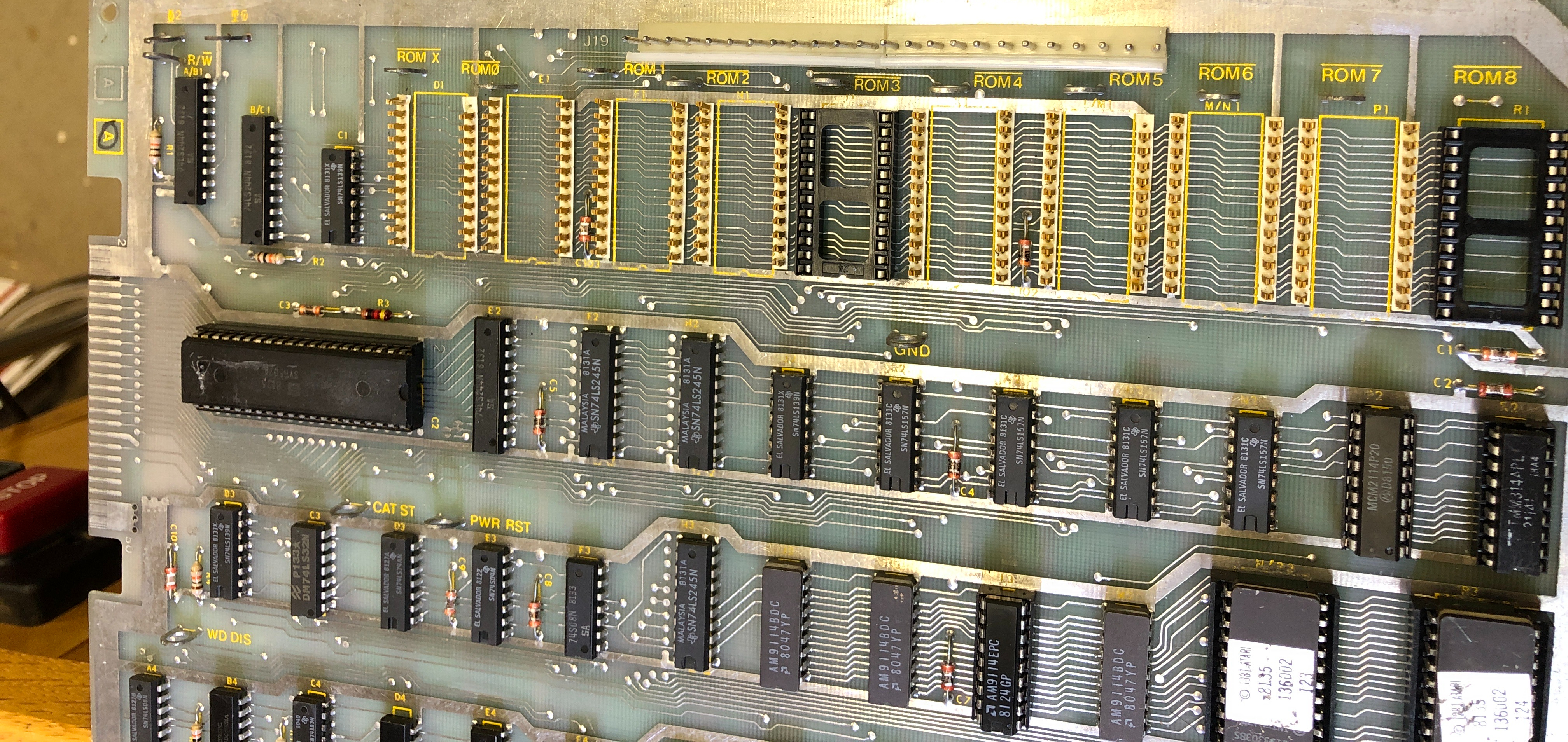
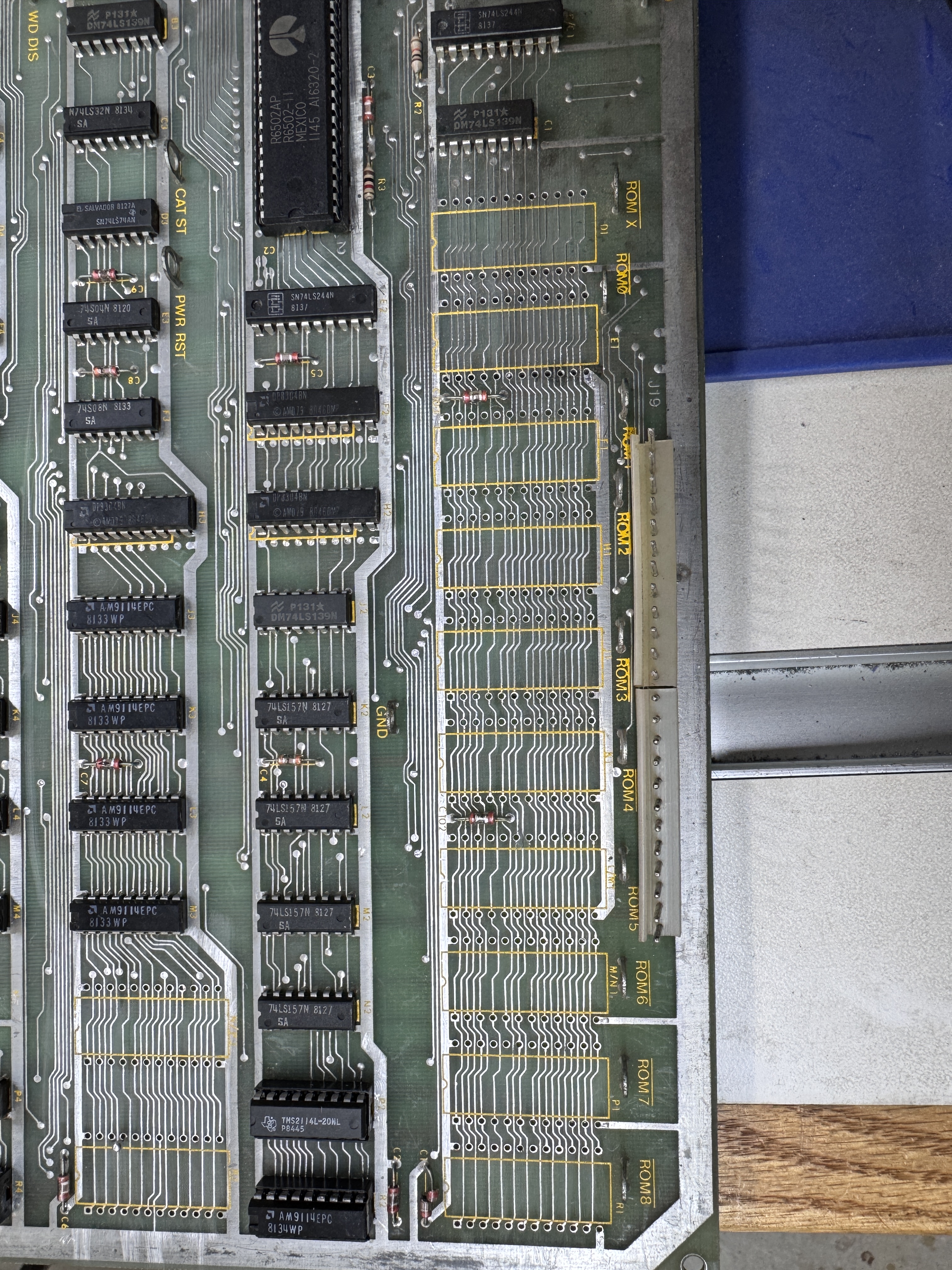
I started on the digital side first. It appeared RAM was checking correctly, but the ROMs were not all reading although they were verified off the board.
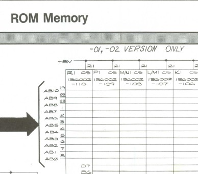
It appeared at first to be this bent chip. Replacing it made no difference however. After further review… It appears this board may have been mid conversion to a single ROM MOD or something?

Jumpers W1 and W2 (set for a V3/4 board set had been moved) This is a V2 ROM configuration. Moving the jumpers to W3 and W4 got all of the ROMs reading correctly.
Once that was done – the vector generator was dead. This turned out to be a broken trace that was under the LS139@B3. It was a microscopic fracture that wasn’t visible when I replaced the chip.
Two of the missing caps were a bit obscure in that I never have to replace them. Had to wait for parts to come in to complete the repair.
Board works!
Board 7 – Board in for repair
Initial Inspection:
- Missing DAC @B10
- Missing state machine PROM @D7
- PCB Reset button is missing
- Unsoldered legs @E6
This particular board was also one where someone else had started but never finished repairing it..
It is a very early Tempest that used the MC3410 DAC vs. the AM6012 DAC. It had been “borrowed”. Searching the net, none of my usual vendors had them. I’d considered converting the board to 6012’s, but there again were a bunch of parts required to do that. I eventually found some on eBay from a vendor in Israel. It took over a week for them to get here (which is pretty good considering..) But they worked.
Replaced the missing PROM.
These repairs plus the full cleaning cycle pulling chips, cleaning legs got the board working.
Board works!
Board 8 – A friend sent me a board for repair
By far the most prior work I’ve seen on a board.
Once I got it on the bench.. I hooked it all up and ran for 12 hours without resetting. I was shocked. The reported problem was vectors not closing/distorted.
I did RAM/ROM checks and they all reported good. I went over the board under the magnifier with a meter looking for open connections and shorts and inexplicably could not find any. It appears someone shot gunned this board and someone else came in after and went over it.. There are many scratch marks between traces making sure there are no shorts, etc.
Here is what happens when you shotgun:
There are 65 socketed chips that are not EPROMS or the CPU … YES 65! In contrast – there are 42 chips that are not socketed as they would have been from the factory. How most of the original RAM survived not being socketed this is beyond me. There is a fair amount of hackery on the front and back of the board. It truly is a mess.


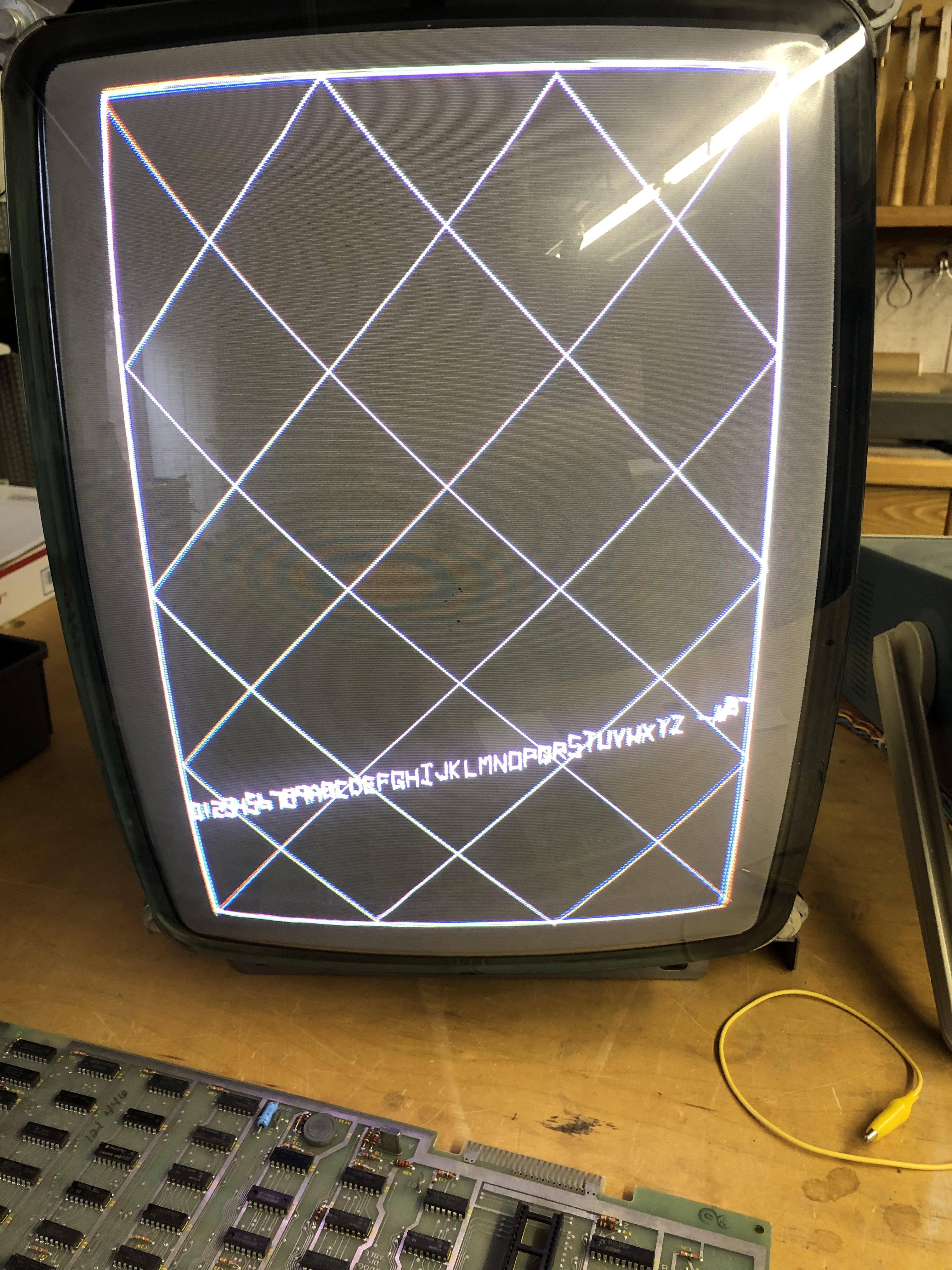
I was convinced I’d be chasing something in here for a while. It’s worse than these pics show.
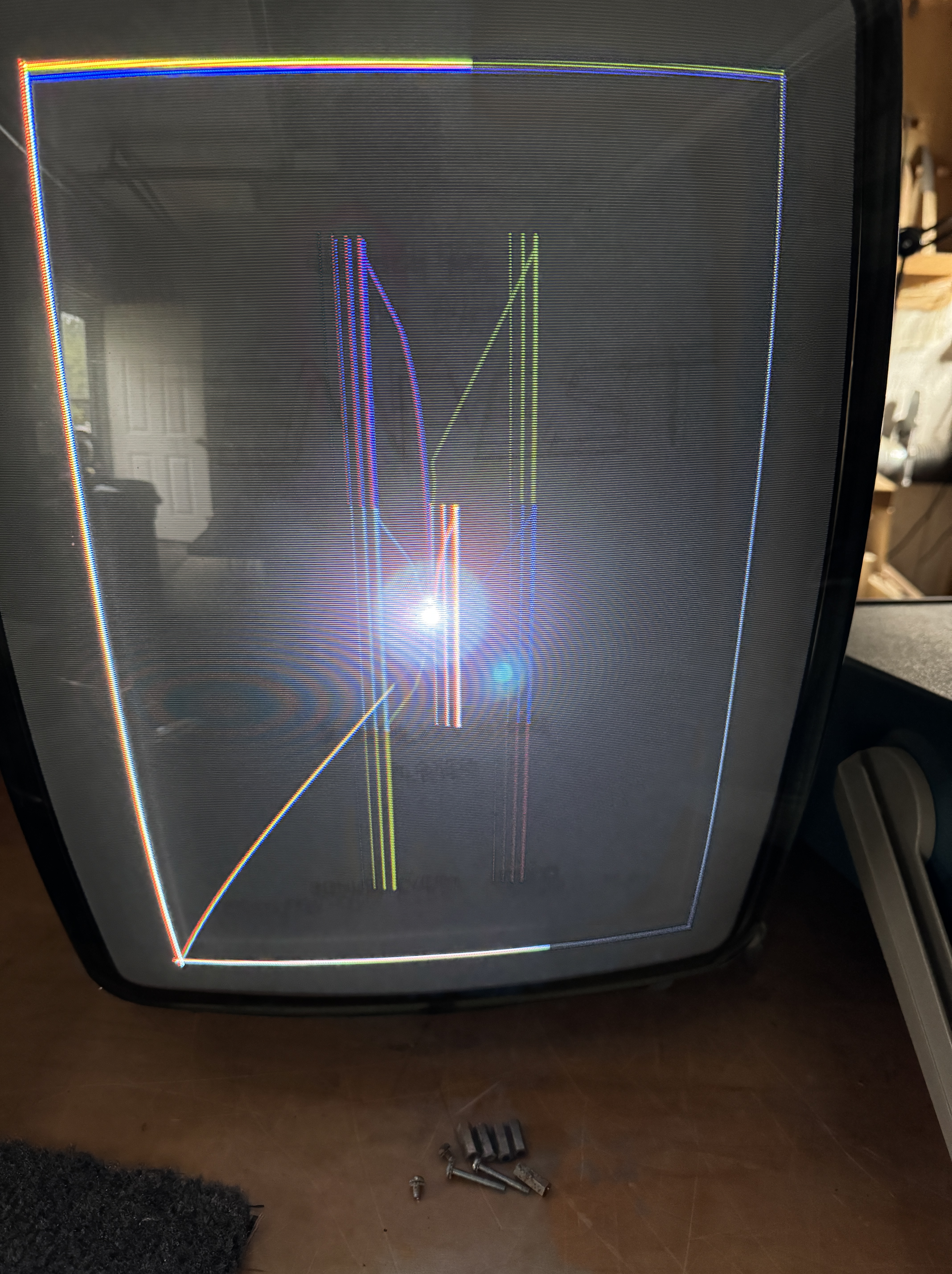
On the screen – the crosshatch made it look like the X-BIP could not be adjusted enough (I adjusted the brightness to remove the blue vector afterward)

However this screen was the most telling:
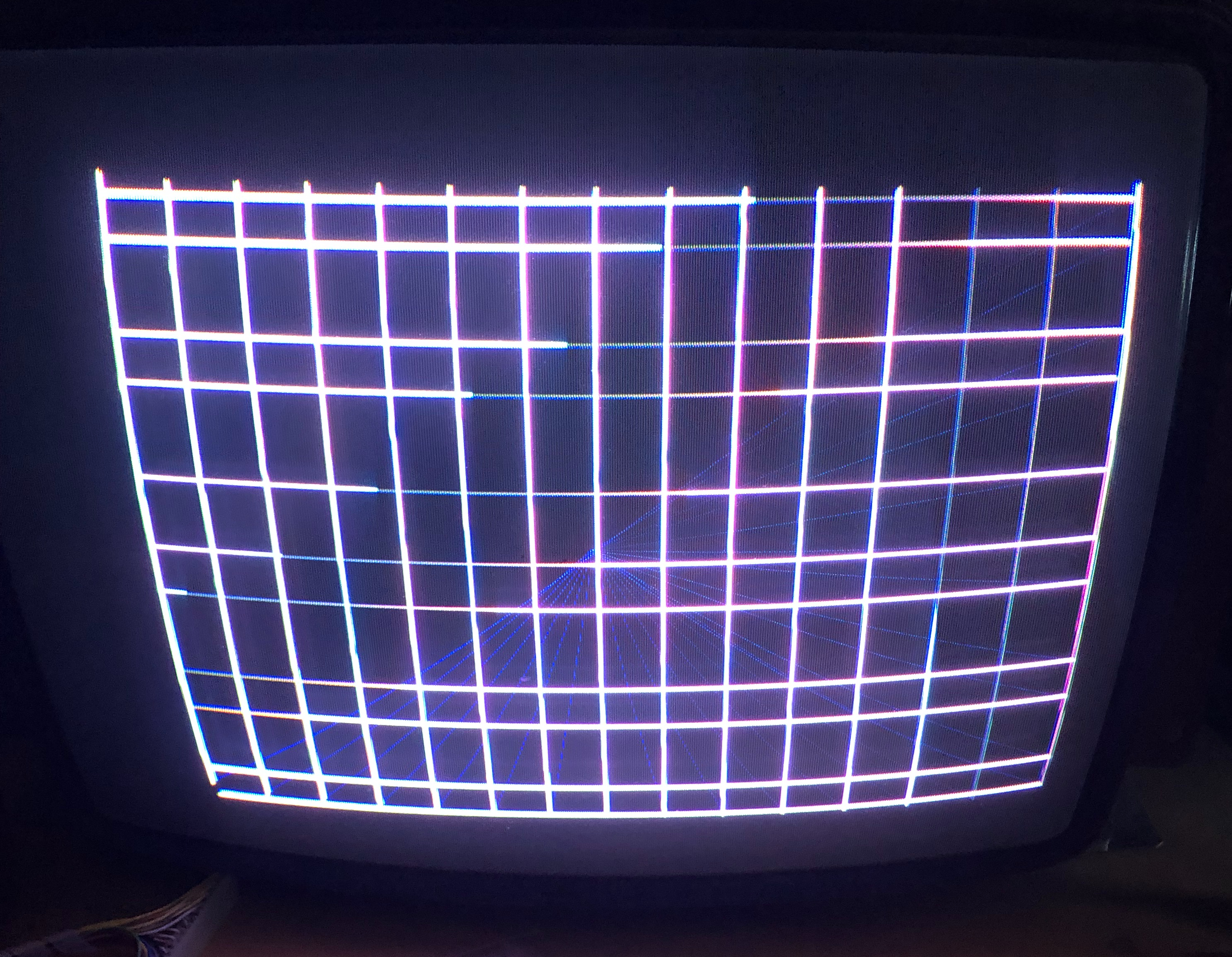
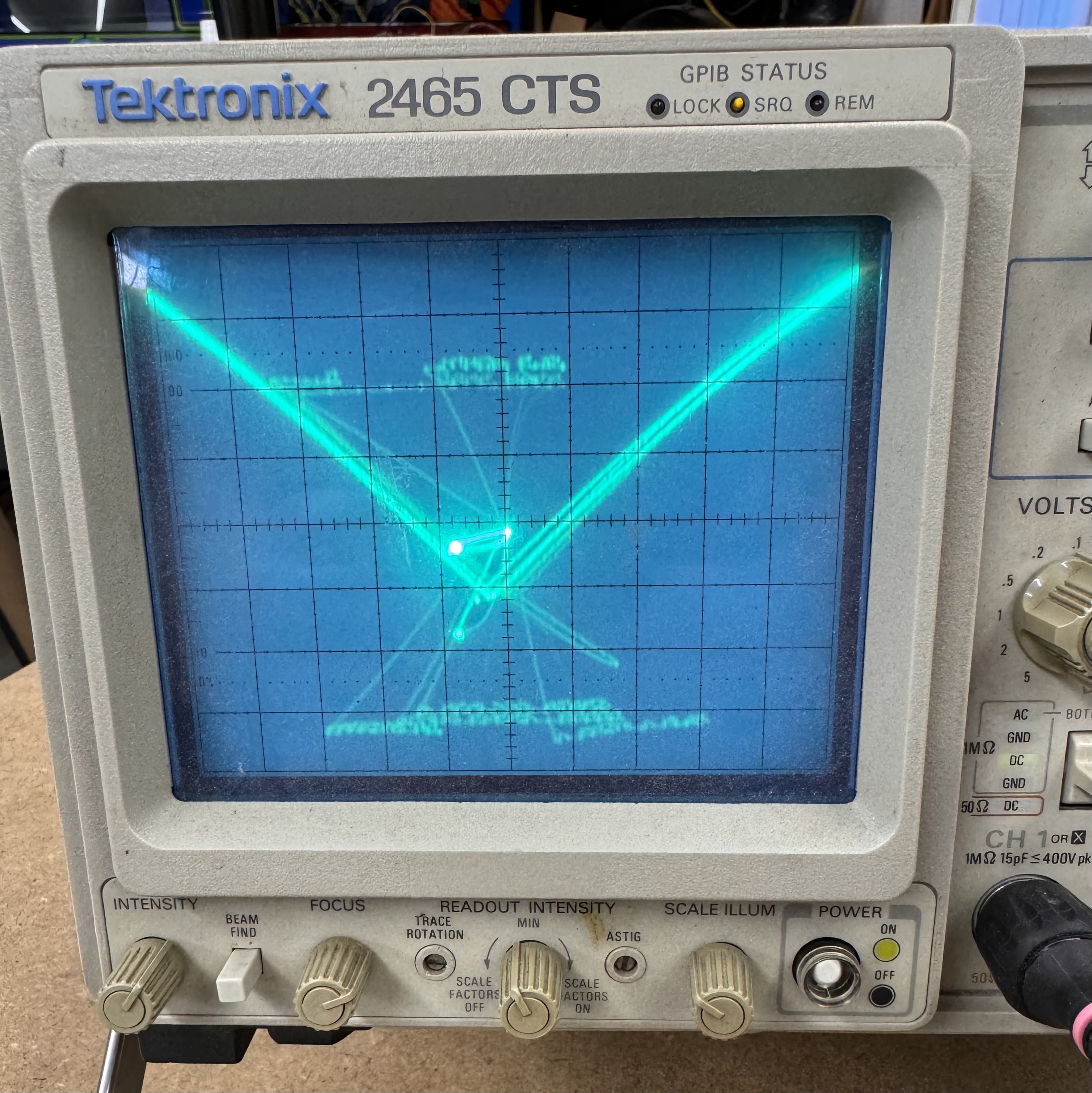
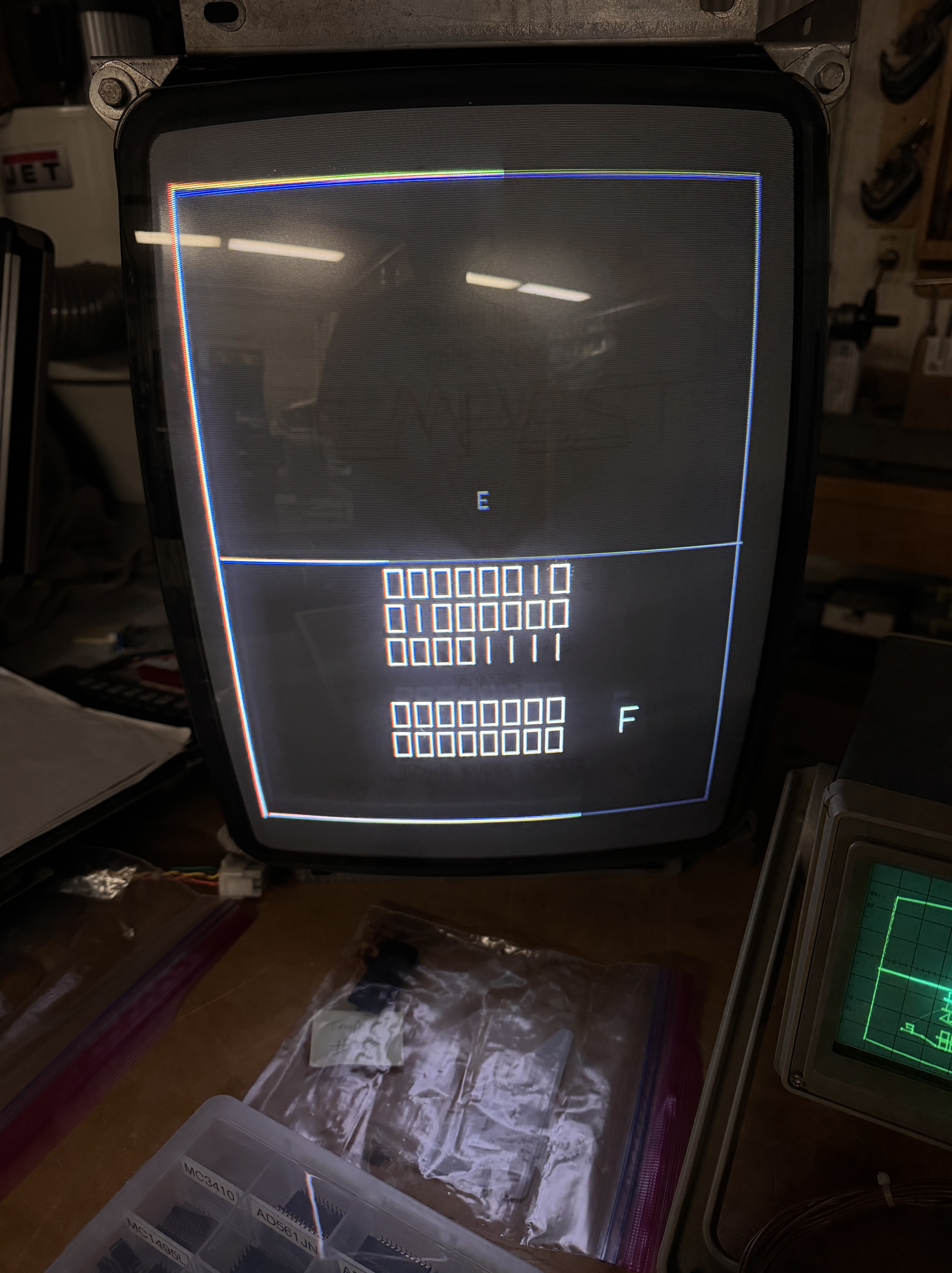
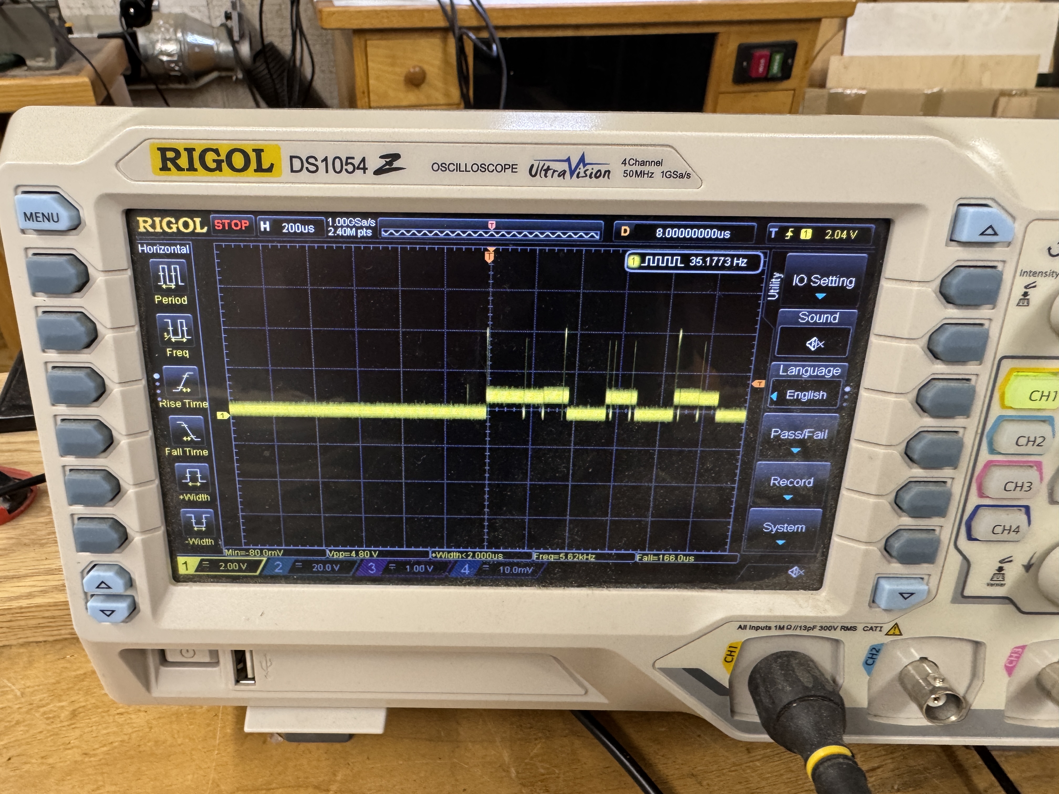
All of the X lines are perfectly straight – but in the wrong place. I surmised a bit was missing going to the X-DAC. The scope showed all of the DVX bits active in the data shifters.. hmm.. Then I came up with an idea.. Use the FPGACatbox and draw vectors toggling each bit.
So I tested X=0, Y=200 on the scope – then X=2,4,8,16 to trigger each bit. All of them moved the beam as expected except 8. 8 moved the beam back to zero. Theory confirmed! Except the square wave signal was there on the shifter and on the DAC.
As it turns out – the X-DAC was bad. It was somehow sending -13v back down DVX6 and killing the ‘8’ bit .. I’m assuming like a pulldown resistor since I could see a perfect square wave on the shifter and the DAC? I had swapped the DACs in the beginning – but must have missed something? My plan is to replace socket the DAC was in.. just incase something is going on under it.
Inexplicably it wasn’t prior work?!

Board works!
Board 9 – Board in for repair
Initial Inspection:
- Connected to test harness – no video output.
Went through and did full board maintenance
- Removed all socketed chips, cleaned legs, Deoxit
- Washed board, Deoxit all sockets
- Clean edge connectors
Once it was all back together – determined that video was getting to the first output stage past the DAC’s. All of the original adjustment pots were pretty smashed up. Replaced all the pots with sealed Cermet pots.
Board ran for 10 hours.
Then the X-DAC failed. Replaced DAC
Board works!
Board 10 – Board in for repair
Initial Inspection: Needed a lot of work before even trying to power it on..
Here is where it started:
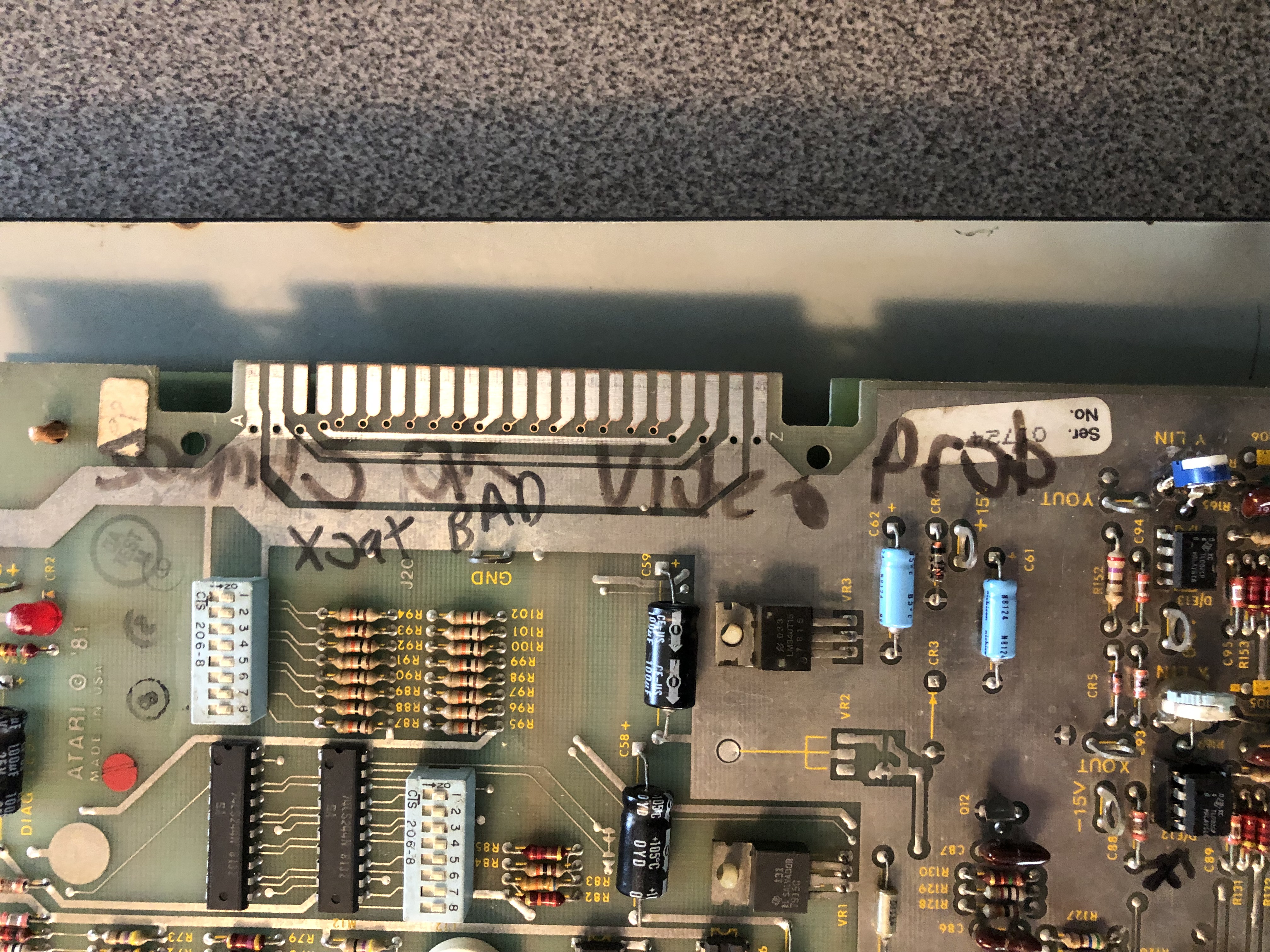
Sharpie writing no video, bad XOUT. The tin had been sanded off the back fingers. I can’t even figure out how the PROM socket got like this.. half of the gold fingers are inside the plastic housing and half are on the outside. Some corrosion around the ROMs. AUX board has bad cold solder joints and many of the pots in the analog section had these weird POTs hacked onto the board.

Other notable items:
- AUX board said some sounds low
- Found a cut trace on the back under @H6
It took a while but I worked my way through all of these initial items
- Replaced all the POTs with sealed Cermet pots
- Repaired cut trace
- Replaced PROM socket
- Removed all socketed chips, cleaned legs, Deoxit
- Washed board, Deoxit all sockets
- Removed all tape, tape residue and used Acetone to remove all of the Sharpie writing
- Cleaned edge connectors
Upon first power up:
- Bit 0 of RAM @L3 showed bad – not a common failure. I usually lose all the bits, not just 1.. I did a quick piggy back to be sure. RAM was bad. Socketed and replaced.
- So far I’ve replaced the sockets @J1 and @R1 on the CPU board. ROM issues have seemed to settle – but more to test.
Once the RAM and ROM checked good – I was able to work on the vector generator. Got a good HALT signal, but the timing was off on all the other tests. Determined it was a bad counter LS161@C8.
With the VG running – test mode would cut in and out.. Which has me working through ROM sockets(see above).
Connecting the AUX board – ‘M’ error. I removed and verified all the PROMs and did a full swap of all the socketed chips to a known good AUX board. All were good. I’d also reflowed all of the cold solder joints. Messing with each PROM one at a time – I could get the ‘M’ to go away occasionally. In the end – I replaced all 7 PROM sockets. Problem solved. I’ve had decent success with these gold Atari sockets.. but not this time.
Last issue on the AUX board – The shooter sound is very faint. I noticed early someone had replaced what should have been a .015uf Mylar cap with a .47uf Electrolytic cap – about 31x too big. The important part is that it is directly tied to the output pin of the Pokey. Replaced and proper sound restored.
After another round of burn in testing.. The 10 ROM sockets were still being problematic.
Decapitated. Looks like ROM-X may have had a busted pin? It would have been the 3rd one that way.. Replaced the remainder of the.
While I was at it – I cleaned up the edge connector and retinned it with liquid tin. Which I’ve used a number of times now. Seals the copper and makes the edge look factory original.
*** Burn-in testing in process.
On the 4th day of testing – the high score save stopped working
- Swapped in a new EAROM – no difference
- Tested -28v and it was coming in at ~-9v
- Swapped in a new Zener diode CR2 – no difference
- Removed C20 -tested out of circuit.. no problem
- C16 went bad at some point
New C16 restored -28V
Board works!
Board 11 – Board in for repair
Initial Inspection:
- Both the Main and AUX boards had no prior work except the pin headers had been reflowed
I’m convinced this set failed at some point and got stored. Did a quick power up and had no output.
After a full board maintenance:
- Bad RAM@L3
- ROM good
- Vector Generator good
- Bad Y output – flat line X output on scope
Replaced bad RAM@L3
Replacing analog switch @E11 restoring Y output
Once the board was running, no Fire, no Zap and the trackball was very sluggish.

Fire and Zap are connected to the LS157@D6 – replacing this restored their function.
The other side if the LS157@D6 also got the trackball running at normal speed. However, it was only working in one direction. Replacing the 4584B (with a CD40106BE) restored the trackball in both directions.
Board Works!
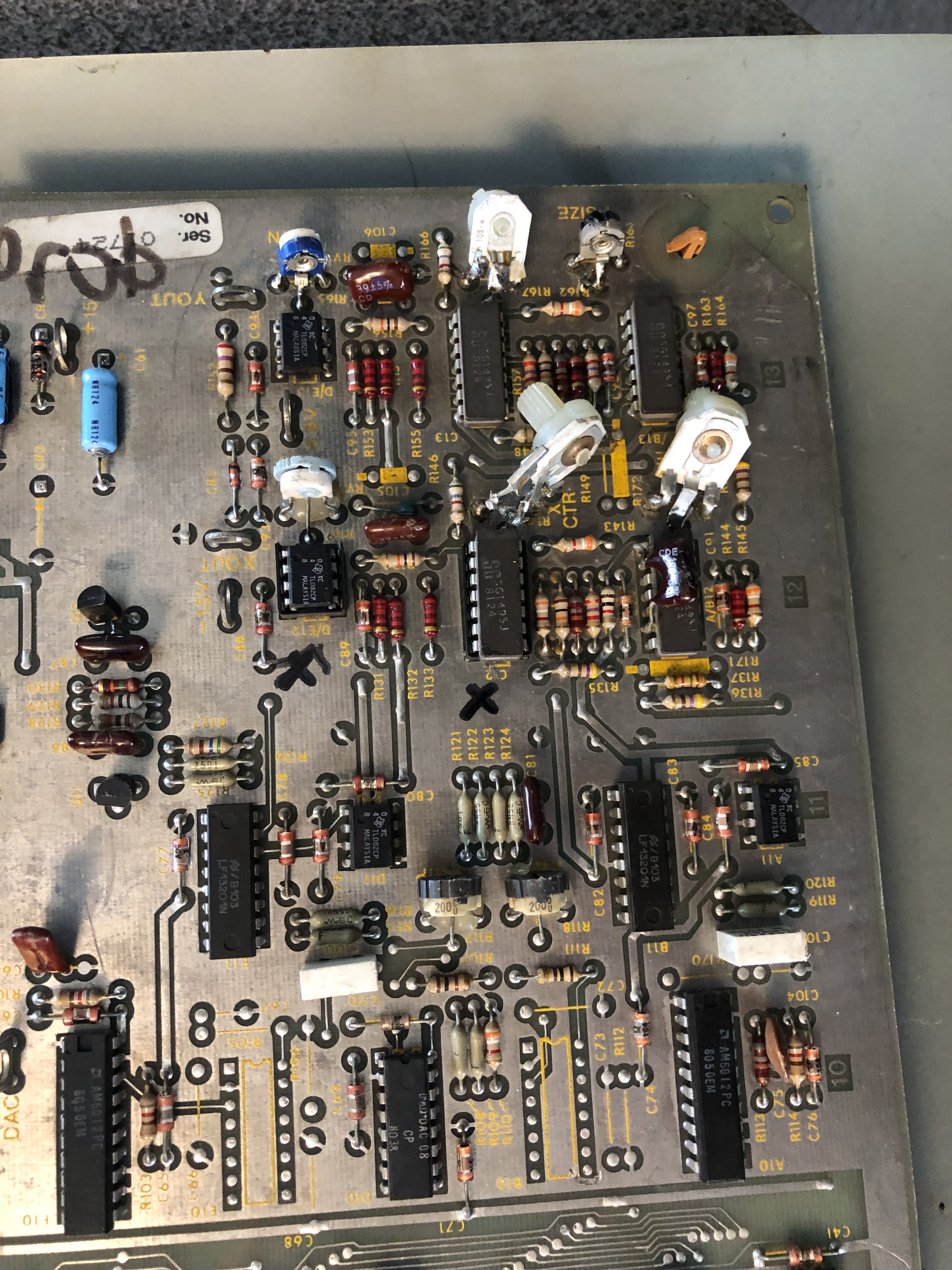
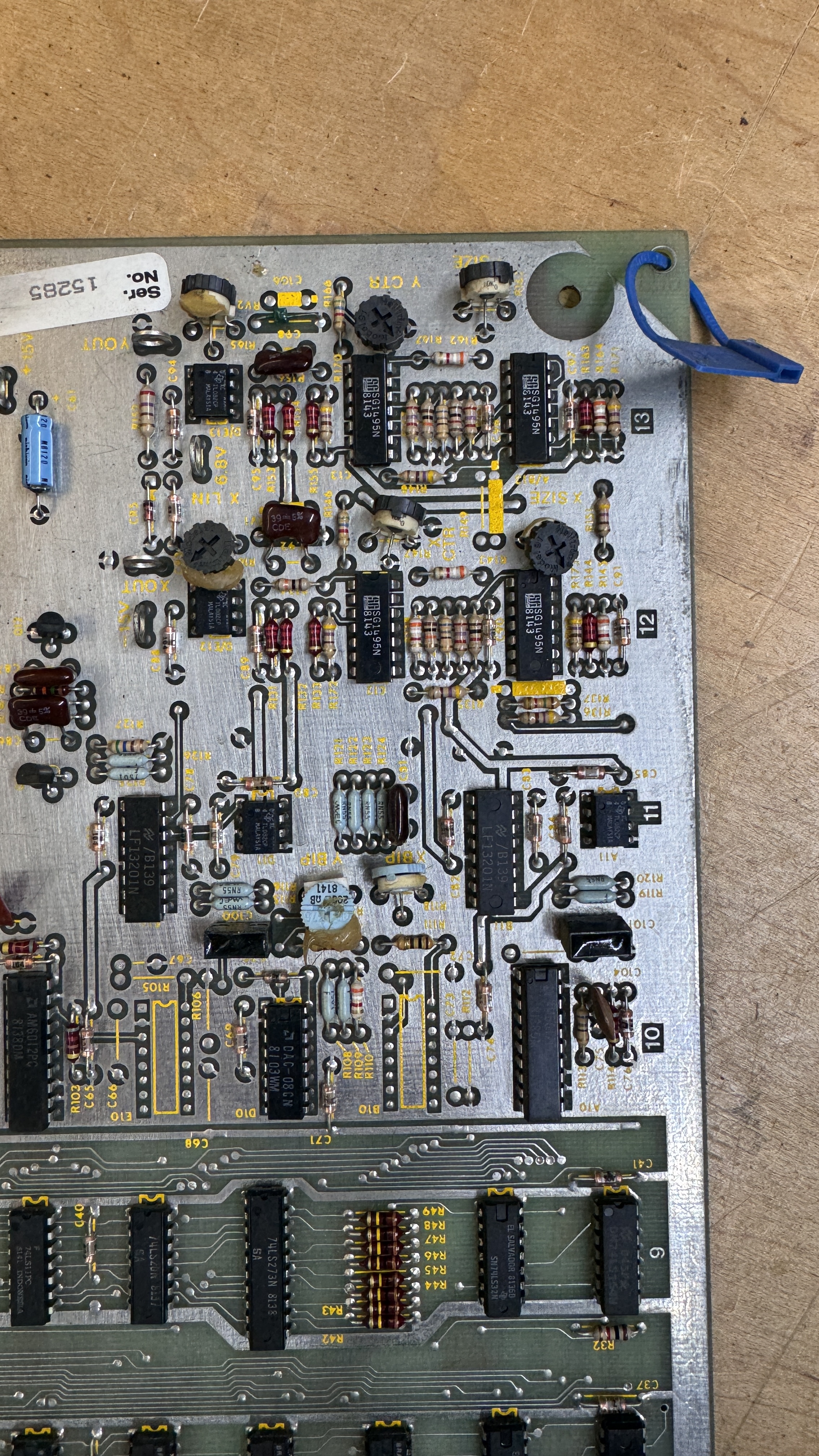
Board 12 – Board in for repair
Initial Inspection:
- Very clean board set.
After a full board maintenance:
- Replaced all of the stand up pots in the analog section with sealed ones

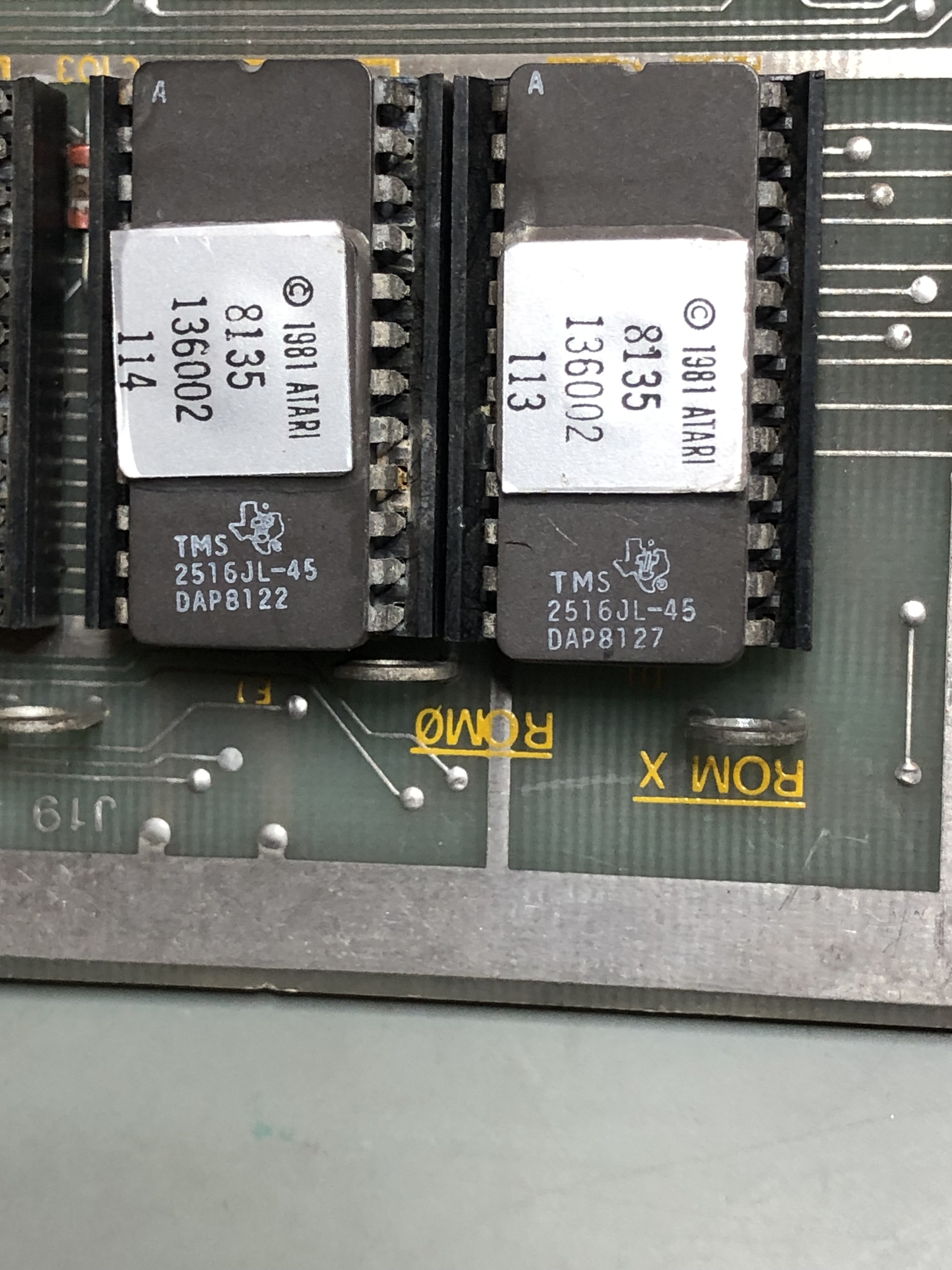
Repaired trace damage under ROM0
Board works!
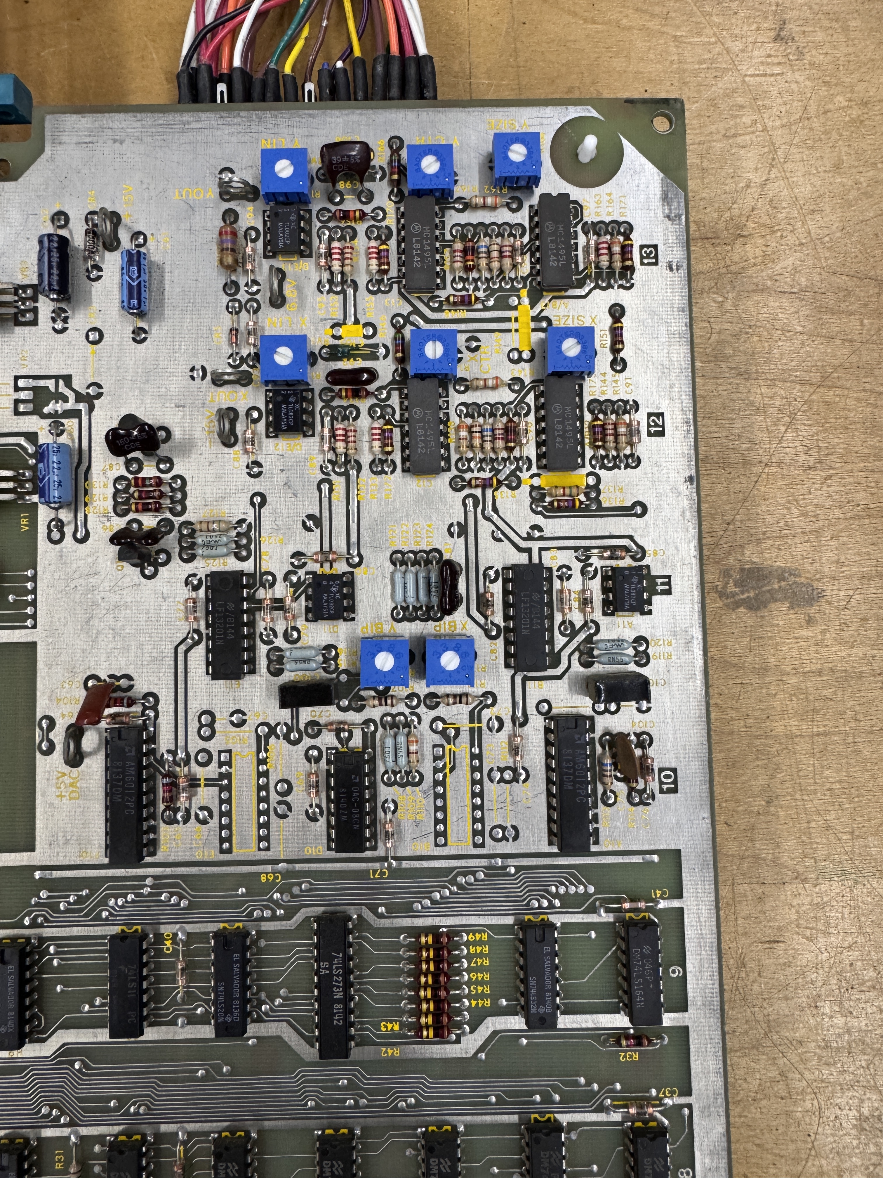
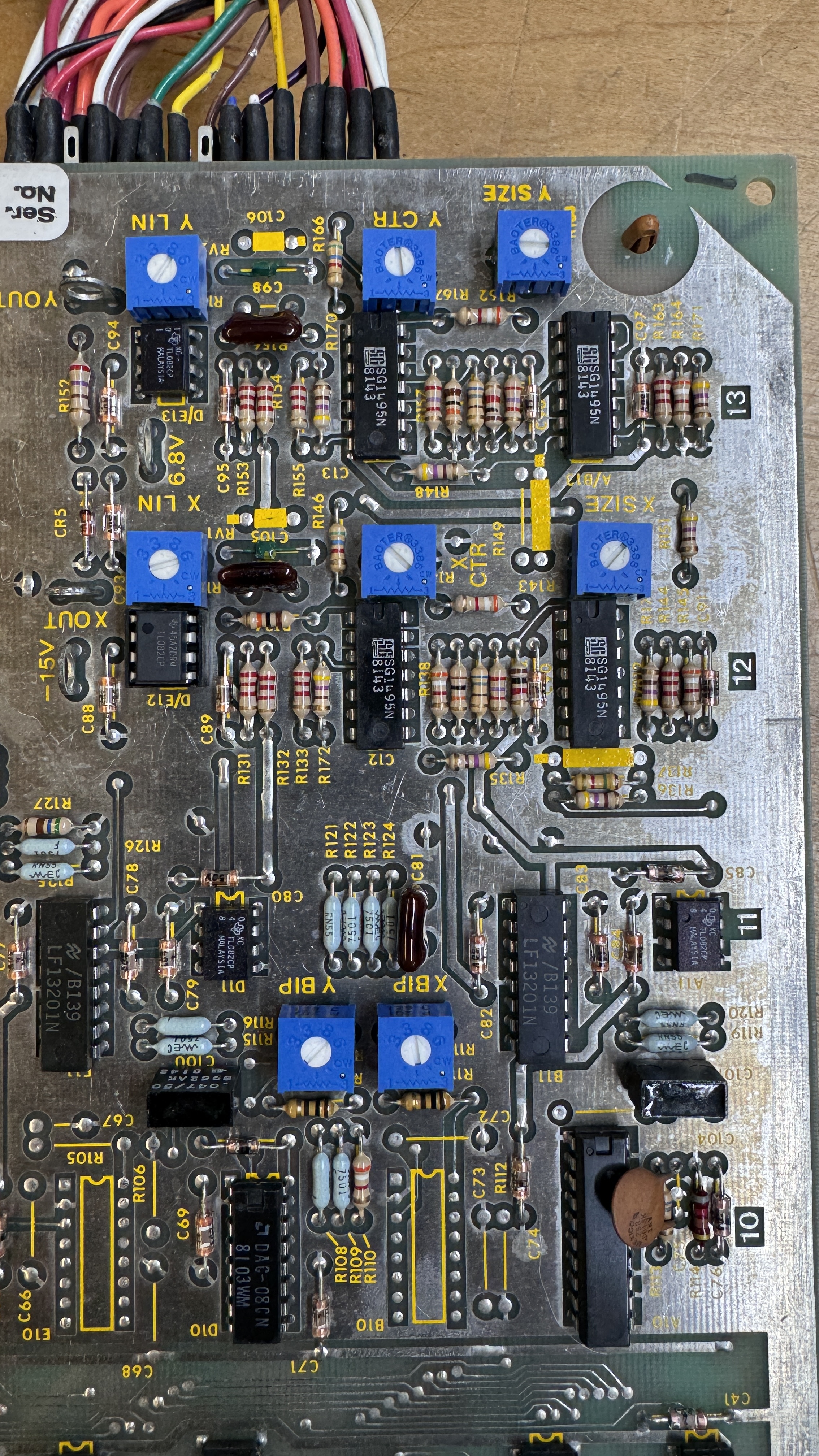
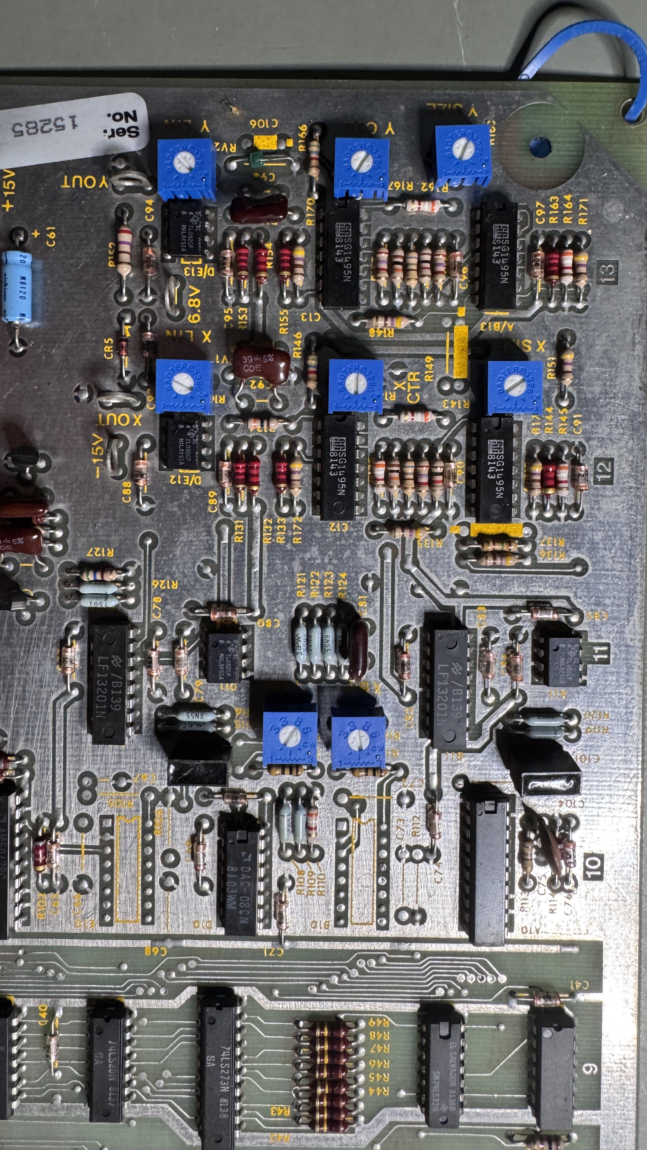
Board 13 – Board in for repair
Initial Inspection:
- Board set had extensive prior work with many issues
- Analog section missing chips
- Missing voltage regulator
- Mismatched ROM set
- Power LED failed
- Traces torn up on many of the removed chips
After a full board maintenance:
- Bad RAM@L3
- Both vector ROM reading as the same ROM
- Vector Generator running very fast
The missing chips had extensive trace damage. To be fair, this particular PCB seemed very sensitive to heat. I had a few pads lift myself. Board came with this half installed broken chip – which was the wrong chip. Finally someone replaced a resistor and left the legs full length on the back? It was the correct value surprisingly.
First up was to get RAM and ROM reading correctly. Replacing the BAD RAM @L3 corrected the RAM issue. The bad ROM was only reading from @R3. It appeared to be LS139@C1..
However – the LS157@K2 was the actual problem. AM12 was not triggering properly. ROM selection fixed. Corrected the mismatched ROM set while I was here.
With RAM and ROM running – the Vector Generator was not running correctly. Pulled and checked the state PROM and it was the wrong one. After reading it – it was BAD anyway.. Replacing with a correct PROM got the VG fully operational.
At this point I had to go repair all of the trace damage and replace the missing chips

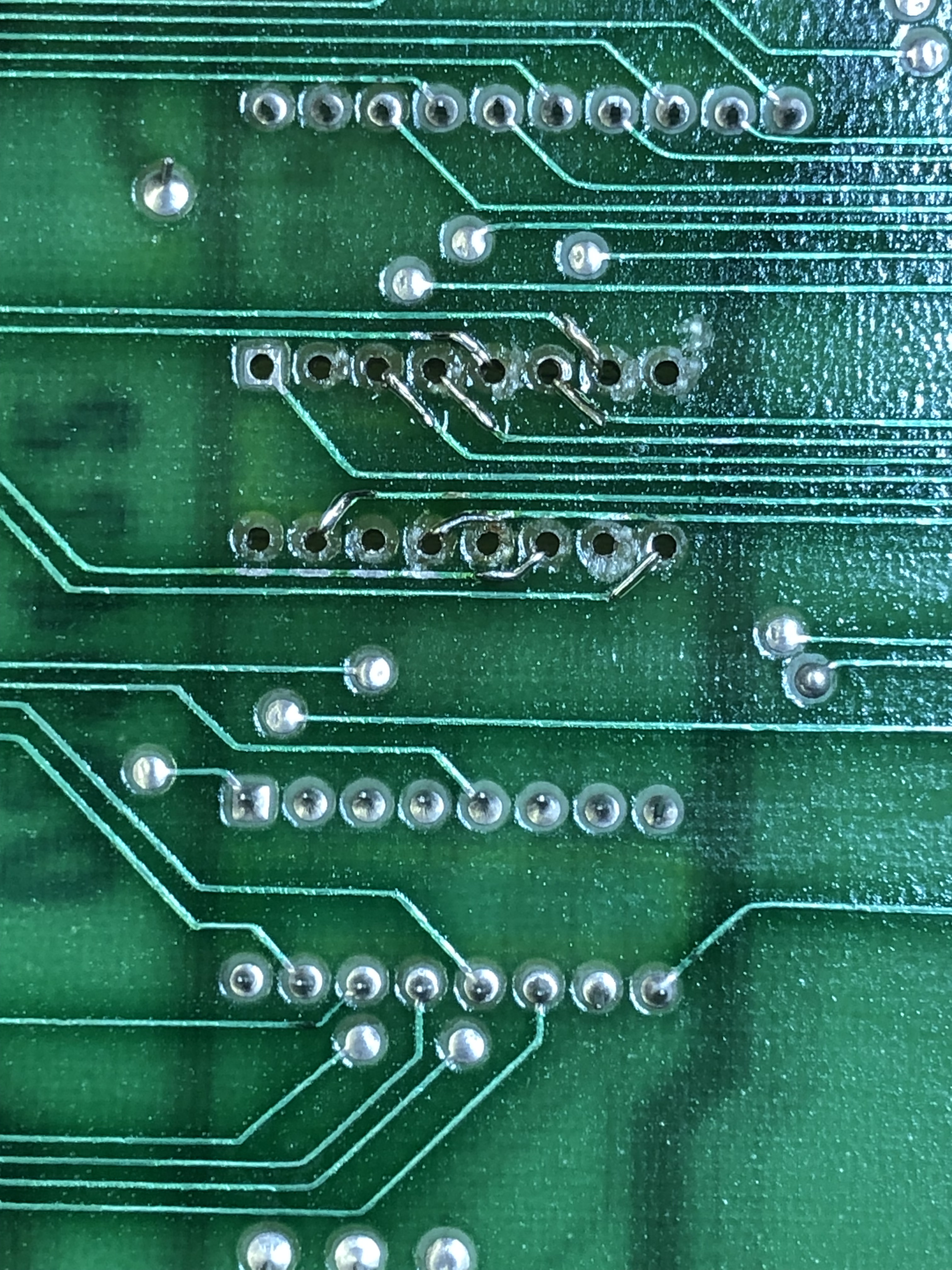

Here are the damaged traces, after cleaning .. I use Kynar wire and feed them through the board and tack solder them in place. After that I use UV cured acrylic as a sealer that holds the wires in place. The acrylic can take the heat of soldering so they do not move when adding the socket. Finally socket installed – A very secure and permanent fix with no jumper wires to snag. It took a couple hours to work through all of the bad traces.
Other items replaced – 15V+ regulator was missing, color RAM @P9 was the incorrect partially installed chip, TL082’s @D/E13, @D11 that were missing were replaced. 1495@C13 replaced. Replaced all the stand up pots with sealed pots. Replaced bad power LED.
Once the analog section was rebuild, analog switch@E11 was bad. All the interconnect pins got reflowed, many cold solder joints.
Finally got the board up and running:
Spent some time working on this one – it appeared to be the LS194 shifters. Clipping a logic comparator to LS194@H5 corrected the issue. Replaced it, no change. I did this a couple times to the other LS194’s before determining the root cause. The odd part was only certain parts of the vectors were jumpy.. Not all of them.

The LS193@C4 puts out multiple clocks. The CPU clock was not an issue. One of the other clocks off this chip feeds the VG (3MHz and 6MHz) and was creating noise and corrupting the vectors. I’m assuming effecting the latch timing?
Replaced LS193@C4 fixed the bad vectors.
Unfortunately there was also a bad Pokey. Replaced that too..
Board works!
Board 14 – Board in for repair
Initial Inspection:
- All original EPROMS
- Very little prior work
- Analog section pots had been worked on, some replaced
After a full board maintenance:
- Replaced all the POTs
- Analog section not working
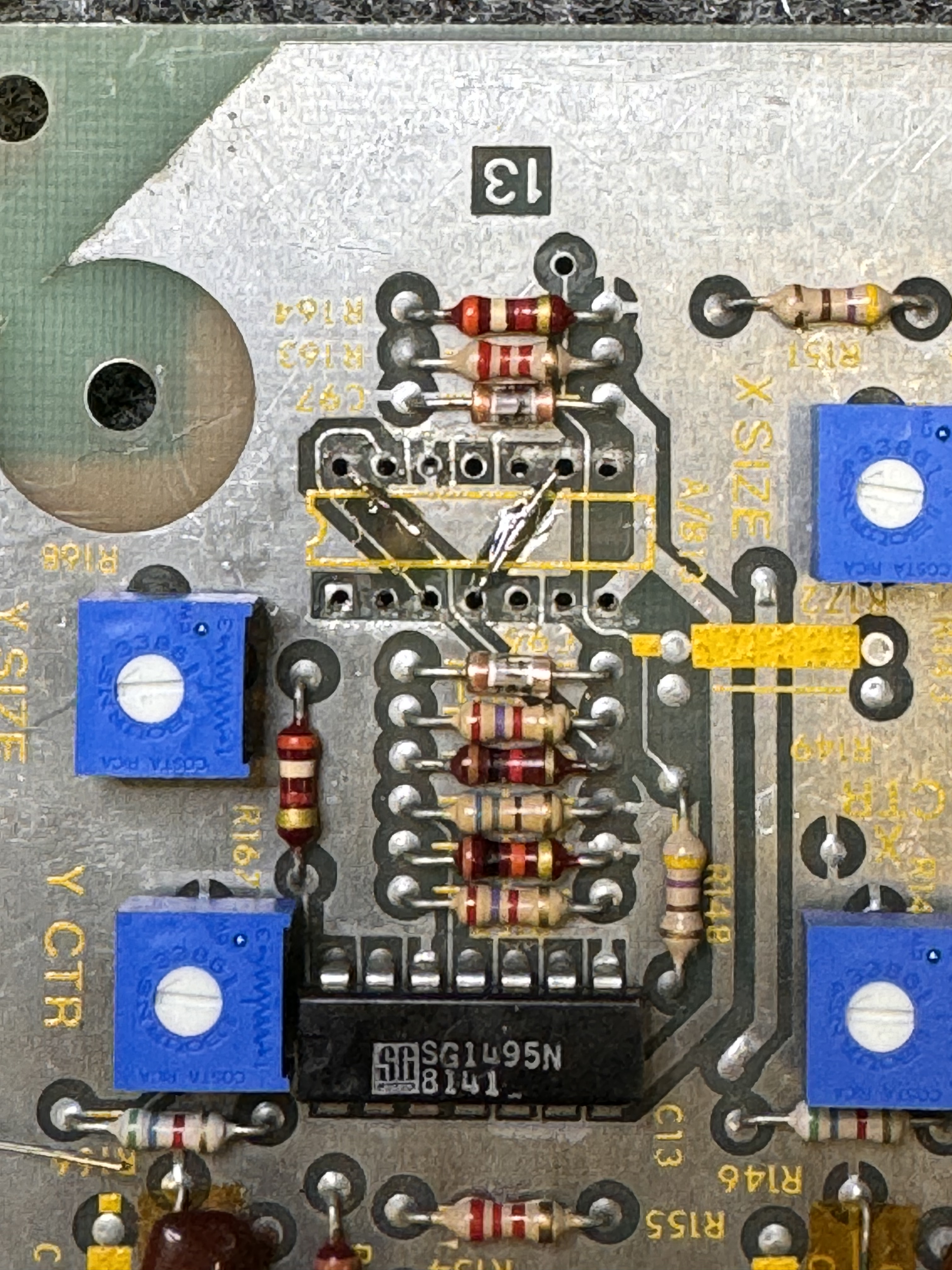
The analog section was not working. After poking around I quickly realized there was no 6.8V getting to any of the four MC1495L multipliers.
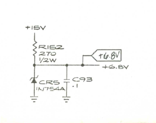
Popped in a new Zener diode CR5, no difference. Unfortunately one of the four ML1495s was pulling down the 6.8v. Pulled one, same… Pulled a second, same… Pulled the third….. third time’s the charm! Voltage restored. Replaced MC1495L@C13. Now that the analog section was fully operational.
Got jumpy vectors as the board warmed up a few minutes.
Easy to locate the chip with some freeze spray. Turned out to be the exact same clock chip as the prior repair, just different symptoms. Replaced LS193@C4.
Board works!
Board 15 – Board in for repair
Received a board – connected it up, seemed to work.
Did full board maint, replaced pots, full test cycle
Board works!
Board 16 – Board in for repair
Initial Inspection:
- All original EPROMS
- Very little prior work
- Cold solder joints
After a full board maintenance:
- Replaced all the analog section POTs with sealed ones
- Graphics glitch
- No controls
Both connectors had many cold solder joints. I’ve started pre-cleaning them with a Dremel and a wire wheel before reflowing them. The solder flows and sticks much better. Graphics glitch was in the analog section. TL082@A11.
Last part was the controls partially worked – but no spinner. Bad Pokey@B/C2 (ouch)
*** Update ***
During the 24 hour automated power cycle test, something failed. The board has already had 2 x 12 hour burn in tests. I’d checked a couple times during this test too and it was fine.. That’s why I run them. I rather they die on my bench.
The Tempest logo and the score table renders correctly.. Need to determine where this went wrong.. Vector ROMs maybe? I reseated the connections and it never happened again.
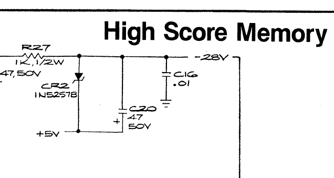
The last part was that it started to lose the high score table – this took a long time just to define the problem. The root cause was just as difficult to determine.
Defining the problem: You could set a high score and run the board for 12 hours and it would be fine.. Then you could come back 2 days later, check it and it would still be there.. Then power down for 5 minutes, power on, and it would be corrupted. It took a few days of EAROM swapping and testing to determine this was a power on/off related issue vs. a bad EAROM issue. In this problem determination – I swapped in known good CPU and AUX boards to help narrow it down to a AUX board issue that corrupted the EAROM during either power up or power off.. It also didn’t happen consistently at power on/off. I couldn’t just flip the power switch on off and kill it. Generally I needed to wait 5-10 minutes.
Finding the root cause:
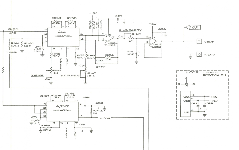
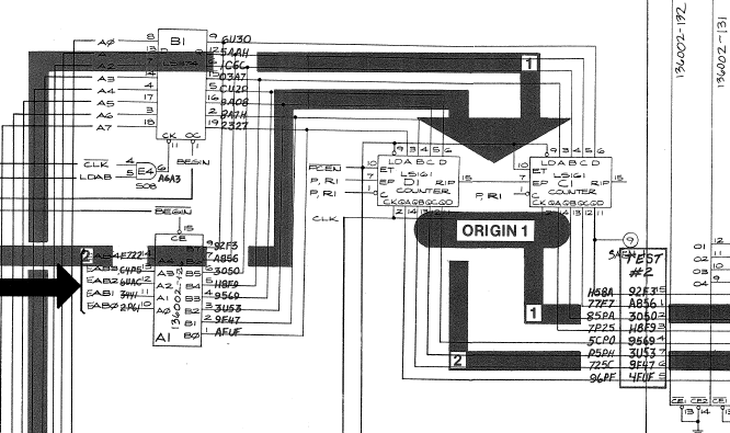
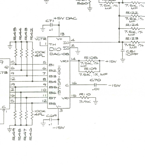
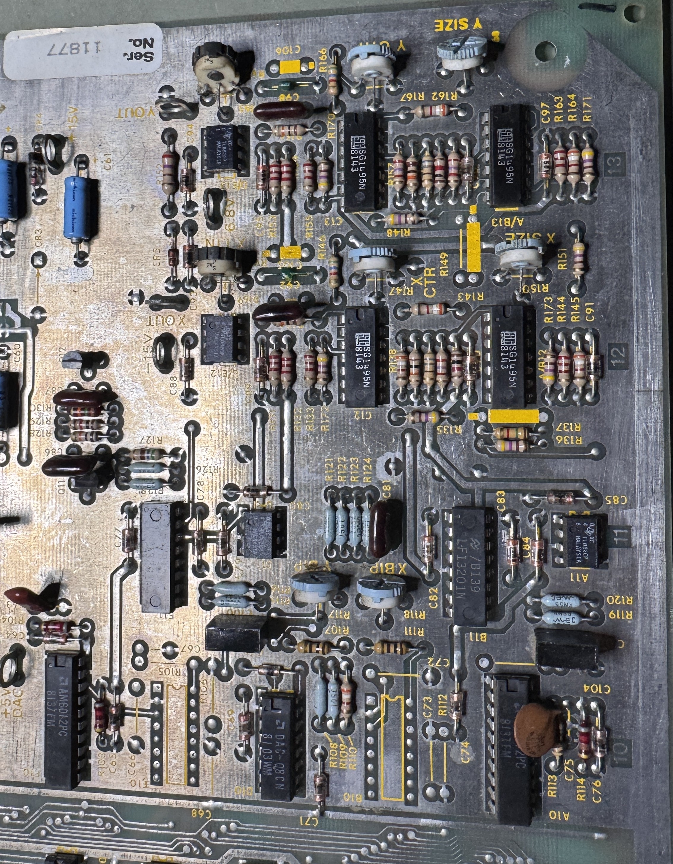
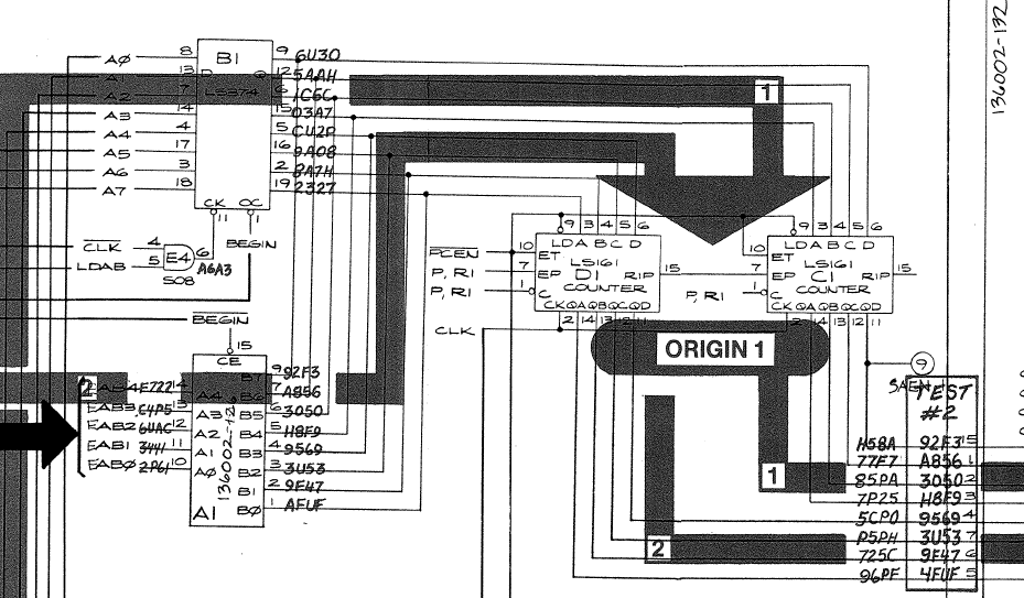
Here is the (pretty much) the entire circuit.
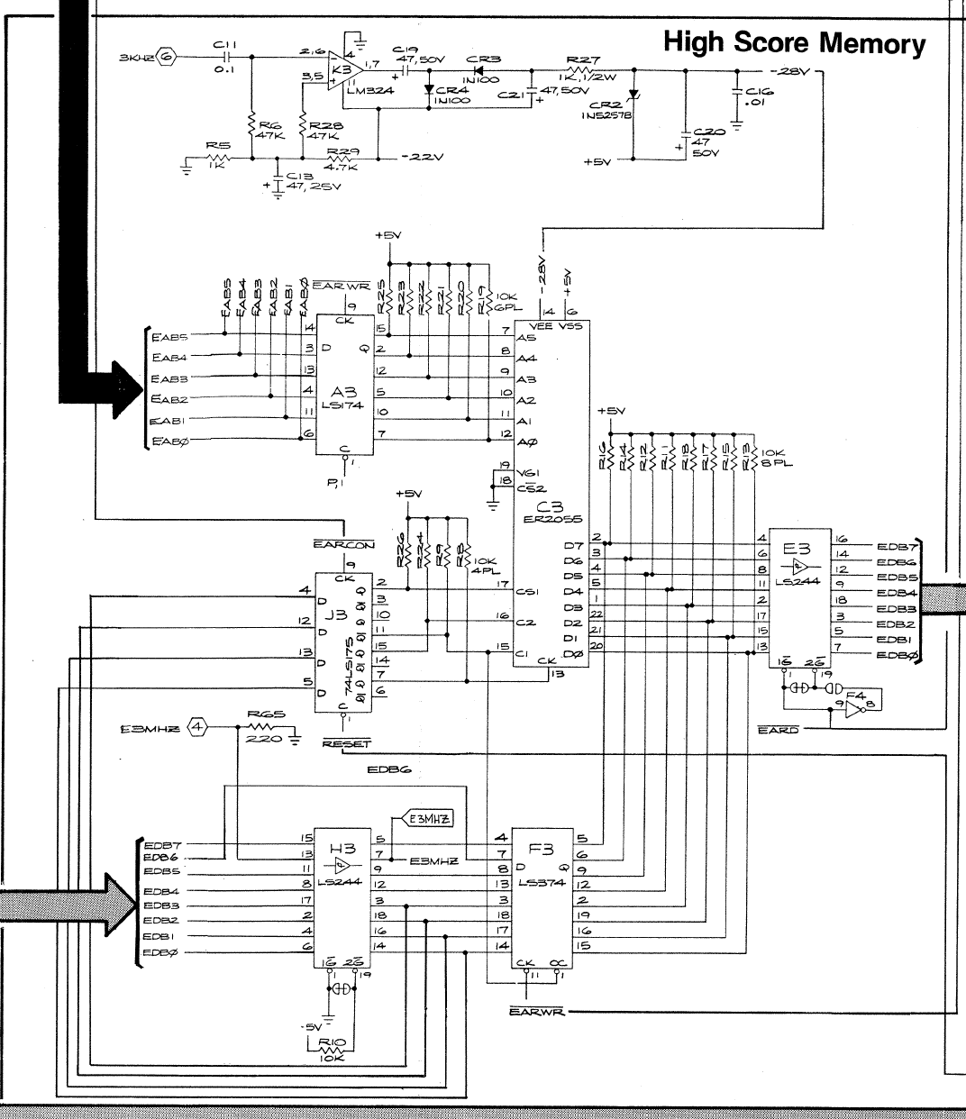
The truth table for the EAROM@C3

For data to get written: CS1=1, CS2=0, C1=0, C2=0 - I tried to see if I could capture this using the scope – but power on/off causes things to jump around and it had to be something that was triggering very fast.
After a lot of head scratching and wasting too much time – I started swapping chips that could effect it: LS175@J3 – no change, LS244@E3 – no change, LS174@A3 – no change. I replaced LS374@F3 and LS244@H3 just because I was running out of ideas.
At one point I was considering the RESET circuit was wonky and held the RESET line low @J3 – no difference.
Looked at the power and I was not getting -28v (getting -26.8 ish) I replaced C20 and CR2 – but it really wasn’t voltage related it turns out. Checked all the pullup resistors between A3 and C3. All good..
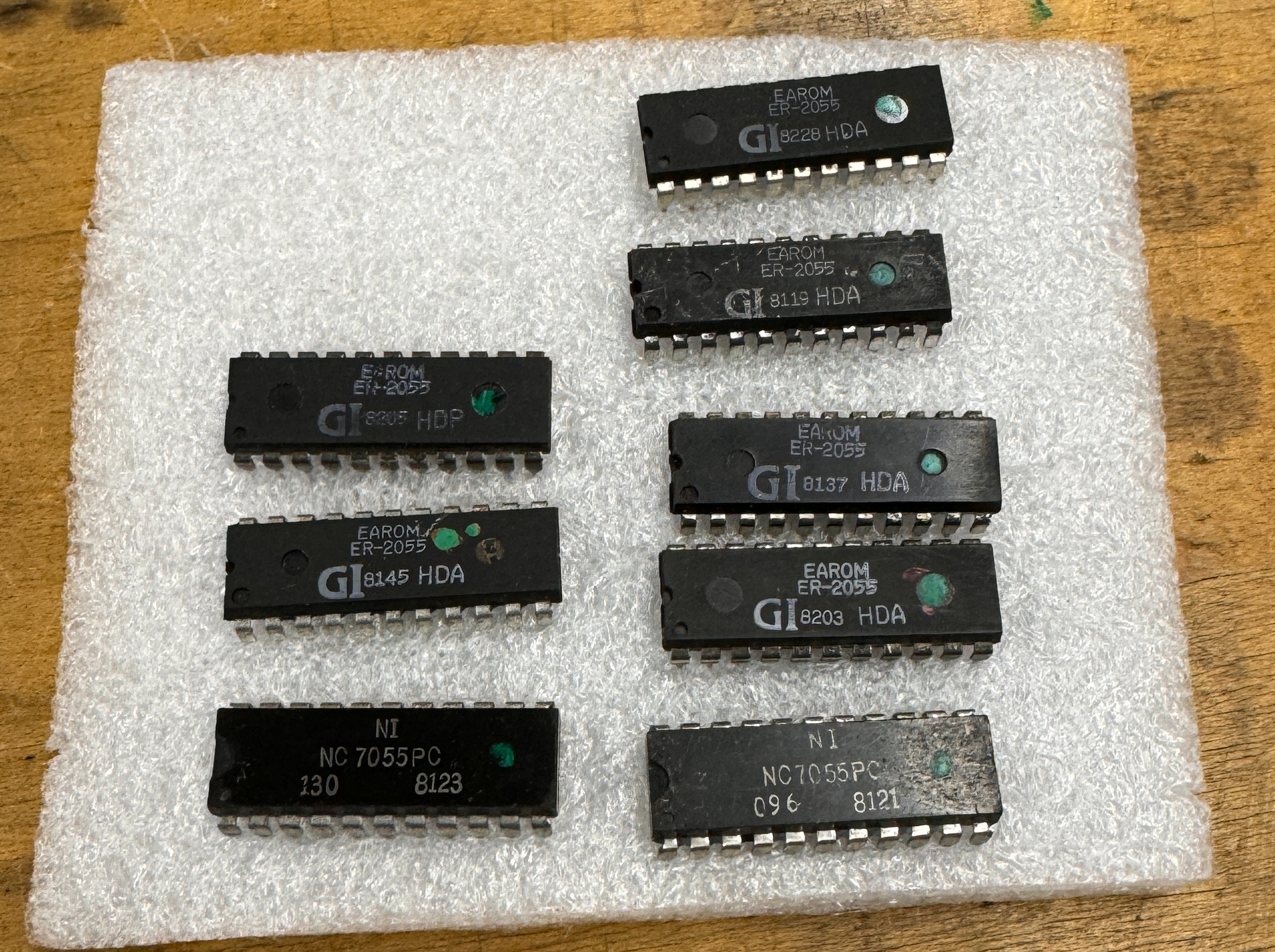
The FPGA Catbox was a big help – I was able to download and check the EAROMS to see what was getting corrupted. Initially it seemed to be a single bit in the first byte, but after a few cycles it seemed to be a bit more random and more than just the first byte. One positive side effect was I programmed all of my EAROMs so I had a good reference point and a steady supply to corrupt and test.
Going back to how the EAROM could get written – the control bits have to be getting set for a split second at power on/off.. The LS175@J3 controls that… backing up..
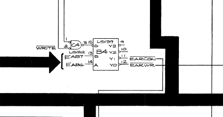
The LS139@B4 controls the EARCON signal and the EARWR signal. Could it be unstable at power on/off? Turns out yes… Root cause LS139@B4 – Just flakey enough to cause random writes. BTW: It was a Fujitsu chip..
Well – this worked for 40 test cycles (10 min on, 10 min off using an automated smart plug). After all that I still had an issue were it corrupted the data.
The WRITE signal goes into the LS32@C4. I replaced the LS32, ran a 30 cycle test (20 min on, 20 min off) and no corruption. Randomly powered on/off over the next few days and it still is retaining the scores.
Board works!
Board 17 – Board in for repair
Chip cleaning is an AM activity…. It takes over an hour to get the main and aux board all cleaned up and ready to test. This set also needed all the header pins reflowed.
Initial Inspection:
- All original EPROMS
- Missing a RAM and a chip in the analog section
- Cold solder joints
After a full board maintenance:
- Replaced all the POTs
- Missing +15V in analog section

A RAM@M3 was missing and the 1495@A/B13 was missing with trace damage. I corrected the traces on the part side before adding a socket.
Once I got it connected, could not read RAM or ROM. Quick inspection found trace damage under the CPU.


Someone got under there with a screwdriver and hacked up AB0 and a couple other lines. Pic on the right is the repaired traces. I beeped them all out. Some are a little damaged, but not broken.
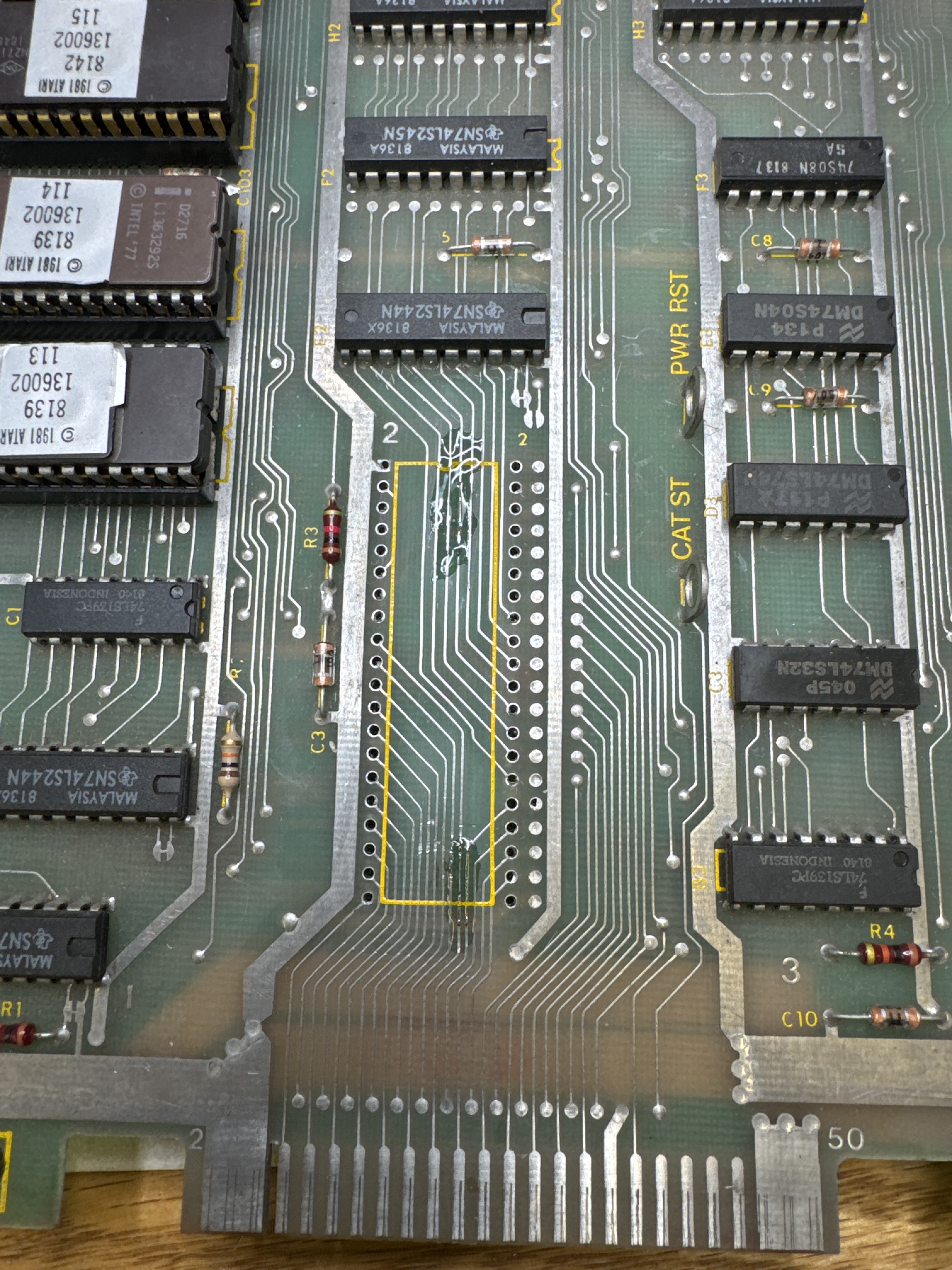
I lock in the repairs with UV Cured resin. Barely noticeable under a new CPU socket. Once that was done..
A single bit RAM error @P2. Not common – usually all 4 bits are bad. Replacing the RAM corrected it. Replacing the 7815 voltage regulator restored the vectors.
Board works!
Board 18 – Board in for repair
Sent in by an operator friend, this one I believe is a backup board. Didn’t test it. Cleaned all the chips, replaced all the pots and reflowed the header pins.
Didn’t retain high score – replaced EAROM.
Board works!
Board 19 – Board in for repair
Similar to the prior board, did full board maintenance which takes ~2 hours including replacing the stand up pots with the sealed cermet pots.
Vector ROM – NP3 was bad – an original mask ROM.
Board works!
Board 20 – Board in for repair
Reported graphics issues
Did full board maintenance which takes ~2 hours including replacing the stand up pots with the sealed cermet pots. Reflowed all the headers.
Bad pots were the culprit on this one
Board works!
Board 21 – Board in for repair
More Tempest graphics issues – performed all the board maintenance. Bad pincushion was the reported problem.
- Clean all chips / Deoxit
- Reflow all headers
- Replaced all stand up pots with sealed Cermet pots
Testing on the bench:

Before and after. That is some serious pincushion.
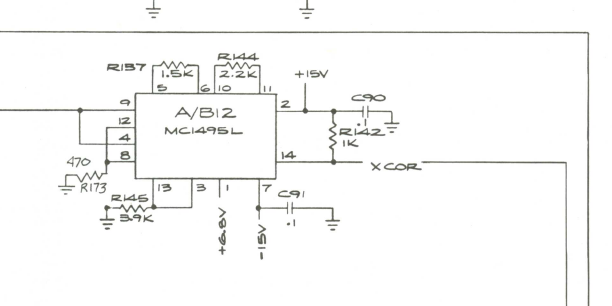
MC1495@A/B12 handles the pincushion correction for the WG6100. Replacing it solved the problem. The interesting part is before replacement – the top horizontal line was perfectly flat on the scope and curved on the 6100. After replacement, curved on the scope and flat on the tube. Makes perfect sense – it was just interesting to see.
Board 22 – Board in for repair
Received a board with some graphics issues. Someone had been working in the analog section and it was a little beat up. Graphics issues was caused by DG201@B11.
Replaced all of the pots with sealed cermet pots. While I was there I did some repairs to make the board more reliable.


This jumper was put in place to repair trace damage on the parts side. The chip was not socketed. I removed all of this and cleaned up the mess. The last pic shows the parts side repair using Kynar wire repairing the trace and locking it in place with UV Cured Resin. Added a socket on top and made this much cleaner.

Typical on Tempest, lots of cold solder joints. The third pic shows the same joints but post wire wheel cleanup and before reflowing. The Dremel/wire wheel combo removes most of the crud so that the joints reflow cleanly.
Board works!
Board 23 – Board in for repair
Received a Tempest – owner told me he had no history and it had been sitting for a very long time.

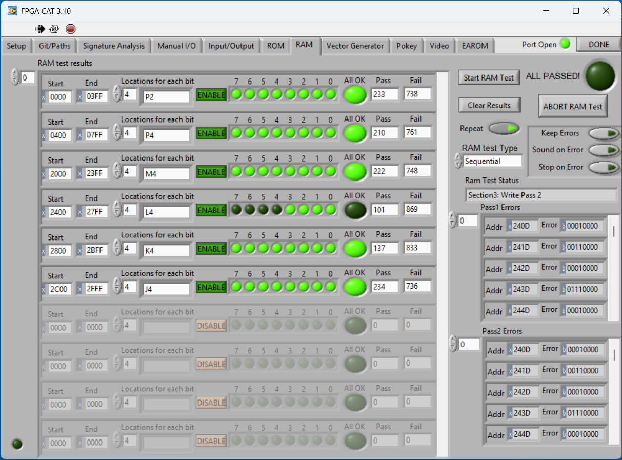
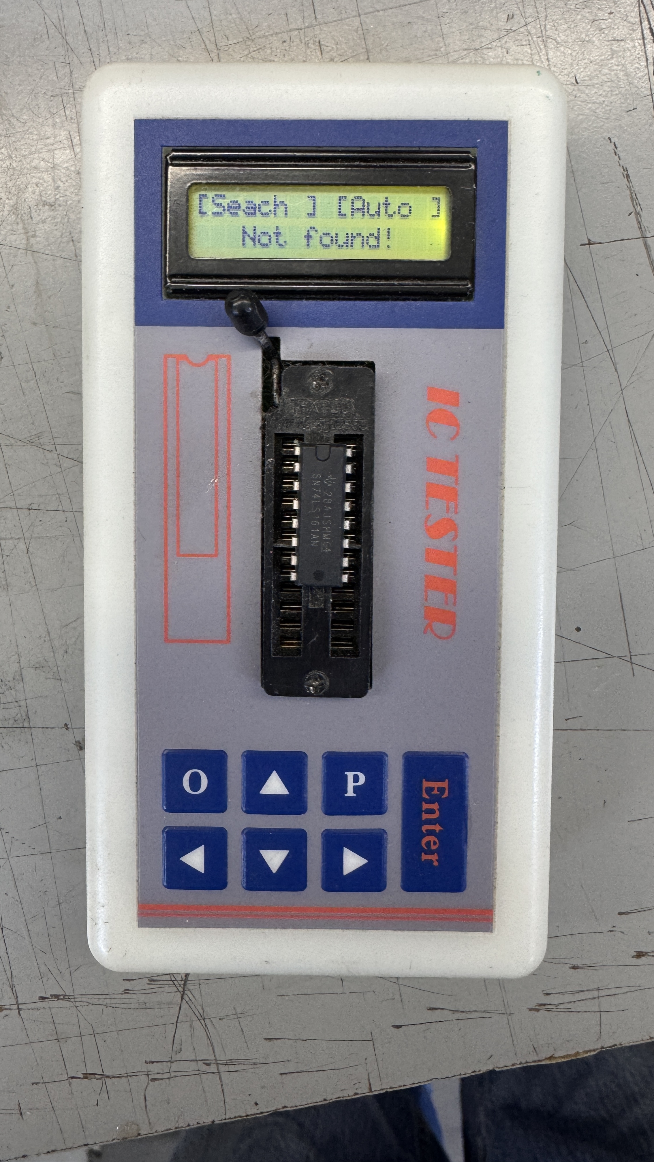
Connected to the tester and here is the memory test. One at a time I replaced each RAM and corrected each issue. I don’t see single bit errors often – but the tester does a great job. No need to count selftest beeps. RAM @L3, P4, J4, K3 were all bad.

Once the RAM was replaced I was able to get a diag screen on the scope – which means I can put it on a monitor.
Had not seen 3 letters at once in a while. Tested the Pokeys – Both were bad. The owner suspected at least one was because we sent a Pokey1 replacement. I have one of mine in the second slot for now. R was from the bad RAM and M for mathbox failure.
I swapped around socketed chips on the AUX board – because it was fast/easy. No difference.
Further inspection showed that the carryout bit -Pin15@D1 was not working. Replaced LS161@D1 to get the AUX board up and running.
Now that it was running – it was not reliable. It kept cutting in and out by pressing on the ROMs. After messing with them a few times, I cut out all 12 of the 24 pin ROM sockets are replaced with dual wipes. The gold Atari pincher sockets can be a bit hit or miss.
*** During testing – another of the RAM failed. 5th of 12. I contacted the owner and we replaced the remaining 7 chips. A total of 12 RAM sockets were installed.
All of the pots were replaced with sealed Cermet pots.
Board works!
Board 24 – Board in for repair
Board was reported to have graphics issues.

One of the first things I do is a close visual inspection looking for obvious issues. Here there is a missing Y linearity pot and a broken Y center pot. These headers had been reflowed, bit they are a bit bubbly for my liking. I reworked them.


I often was dirty boards, there were not bad, but there were bug webs inside – so they got a bath. The legs on the EPROMS were also particularly oxidized and needed to be cleaned.

Tempest always gets a complete set of sealed pots to replace the original stand up ones. After all of the board maintenance, cleaning and adjustments.
Board works!
Board 25 – Board in for repair
Received Tempest for repair. It is a very clean board with very little prior work.
Removed, cleaned all the chip legs. Replaced all of the pots with sealed pots as always. All of the headers also needed to be reflowed. This process normally takes a couple hours.
Once powered on, the board was resetting. Working through the board and the failure it was having, I decided to use the FPGA Tester and do signature analysis on the PCB.

Signature analysis was useful to determine that the PROM@L1 had failed. The Tempest troubleshooting guide provides all of the detail for the 3 modes of SA available. The interesting part was all of the proms provided correct signatures except the actual bad one. The look like they would feed each other bad info.. but that was not the case in this instance..
Once the prom was replaced.
Board works!
Board 26 – Board in for repair
Board got all of the normal treatment as above
Notable items:


The Y pots were completely missing and there were a couple of busted ROMs (115, 116). Cold solder joints prevented the board from running.
High score save EAROM was bad.
After full test cycle – Board works!
Board 27 – Board in for repair


All PCBs start the same way.. remove and clean all chip legs and inspect.. The headers had cold solder joints and the X-size pot had a resistor hack installed. This all got corrected and all the pots get replaced with new sealed ones..
Once powered on, boards passed RAM, ROM tests. Graphics were all messed up. Testing through the Analog section revealed a bad TL082@A11. Once replaced the vectors looked ok on the scope..
However – they were pretty messed up on the screen. Took a little hunting as it turned out. I suspected another failure in the analog section. A broken 3904@Q8 (which was not this visible, it was bent down) was the cause of the messed up vectors.
From here I bench tested the board – it lasted about 2 hours and another TL082@D11 had failed. It looked like the DAC at first because the DAC was showing an output voltage, however it was the amp that failed on the input side it seemed. Ran the board again and it failed again in another couple of hours. This time – mathbox error (M) on the diag screen.
These often take some time to find the root cause. First is to swap all the PROMs and bitslicers. No issues. I also test with a good AUX board to make sure it is not on the main PCB. It is on the AUX board. Often it is a dead clock or some other small item killing the entire mathbox.

This time – it was 74S08@E4. It didn’t fail dead – it failed by passing the signal@pin10 straight through to pin8. This broke the entire mathbox.
Board works!
Board 28 – Board in for repair
Reported symptoms: Power on, board clicking.
Owner said it had jittery text and replaced all the sockets. At that point it stopped working.

This one has made it’s way around with a number of repair stickers on it.. Board looked good (ROM 121@P1 was in backwards). The socket replacement looked good on the surface – very clean work.
Connecting to the tester – All ROM and RAM checked bad. Here is where I pulled all but 1 ROM and continued checking. On occasion a bad ROM can kill everything.. but not this time.
Moving to the RAM testing:
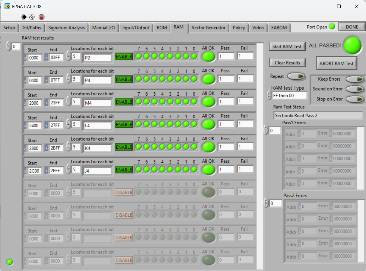
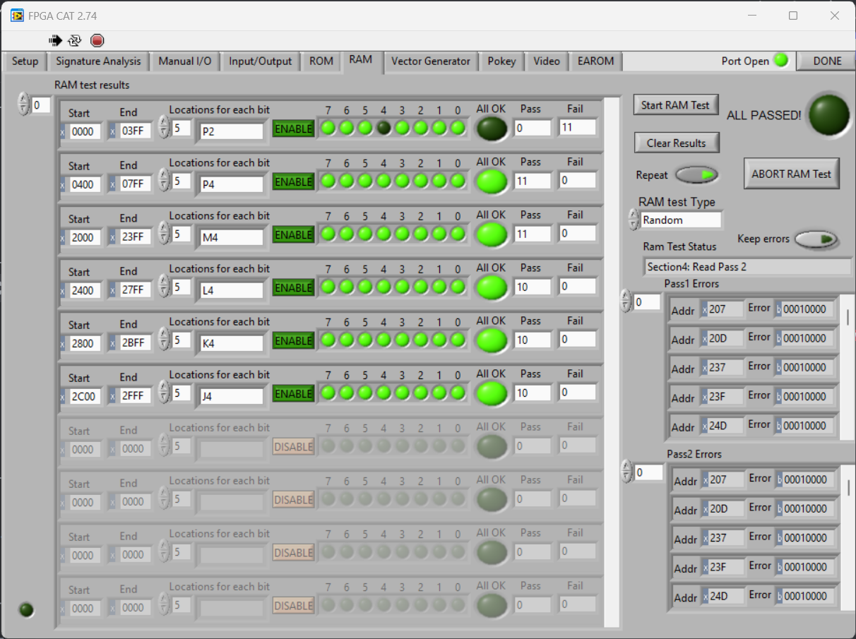
Here is the FF then 00 test – all RAM tests good, right?

Changing just the test to sequential – I can see that the last 2 bits of RAM are showing bad and that starts at address 0x40. A single bit error is showing in the error field.
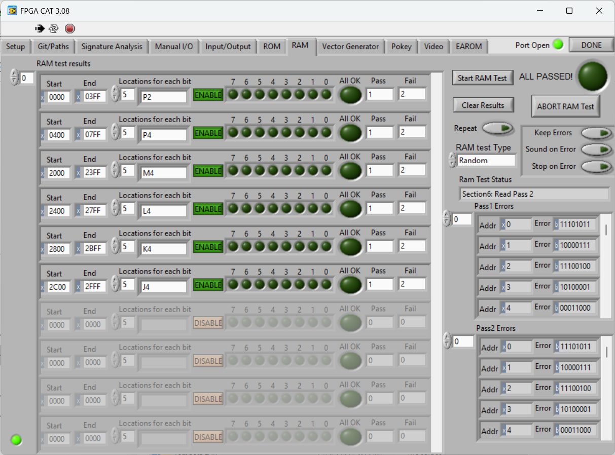
If I chose RANDOM, everything fails – how is this possible? It has to do with the nature of the tests and the data being written, read and addressed. The FF & 00 test writes out 0xFF and reads it back, then 0x00 and reads it back. If the addresses are messed up it doesn’t really matter since all the bits are identical everywhere it is being addressed (incorrectly) and read back. The Sequential test writes sequential numbers addressed in order across the RAM and Random puts random numbers in each byte as it counts.
Using the actual failure from this board as an example: The Sequential test shows the first error at address 0x40.

If I take that number and translate it to the game board using RAM, I write a number to memory location 0x40 in the above Sequential example and the addressing is corrupted – then reading the number back at address 0x40 would have most of the data bits right and the last couple wrong..
The actual issue was AB6 (ROM pin2) was shorted to AB9 (ROM pin 22). This makes sense because the first 6 bits of the addressing on the RAM (AB0->AB5) would be correct and the data errors beginning at 0x40 (which in binary would translate to AB6 being active) is where the data corruption occurred. Hopefully that makes sense..
Now.. the explanation took much longer that how I actually figured it out.. When I see this type of test failure – it is usually an addressing issue and this board has all new sockets. Beeping out the sockets is where I found Pin2 and Pin22 shorted on the ROM bus. However… 10 sockets on Tempest! It could be under any of them. The LeakSeeker comes in handy here. A few minutes of testing Pin2/22 and I determined the short was either under Pin 22 of E1 or Pin 2 of D1. They are directly adjacent and it was a coin toss. Pulled E1 socket.. nope.. I usually lose the coin toss. Pulled D1 and the short cleared just by removing the socket. Put them back and address bus errors all clear!
From here I determined that ROM 120@M/N1 was bad.. odd.. since it was not the one that was in backwards. Also RAM@P2 had a single bad bit.
The bad news is one of the Pokeys was bad.. after fixing all of this..
Board works!
Board 29 – Board in for repair

This one came in non-working. It was clean in that it appeared to never have been worked on, but it was overall pretty dingy and needed to be cleaned up. The original pots had been removed at this point.

Part of the issue were these cold solder joints, they get wire wheeled and reflowed. The set also got all of the chip legs cleaned, sockets Deoxit, etc..
Once up and testing – board had a RAM issue.
RAM@R2 showed bad, removing it showed corrosion on Pin3. Clearing that it still visibly looked ok – but it was not connected. I repaired the trace. Being on the edge of the board, it must have got splashed with something years ago..


Stand up pots always get replaced with sealed ones in the analog section.
Board works!
Board 30 – Board in for repair
This one came in and it worked when I connected it up to the test rig. I believe it has been on a shelf for a while and the owner asked that I do standard board maintenance.
Turns out it could have used it. The socketed chips were all a bit ‘crunchy’ as I describe it. Flexing the board you can hear the creak and crack sounds. Removing them, cleaning the legs and Deoxit creates a cleaner contact and adds just a bit of lubrication. I also replace all of the stand up pots with sealed pots.
Also as is common on Tempest, cold solder joints. Performed full 30 hour burn in testing spread over 7 days and my post repair checklist.
Board works!
Board 31– Board in for repair

This one I powered on and it was actually putting out some vectors, but clearly had issues. Once I know what I’m working with they all get the same treatment – inspection, chip cleaning and removal of the old standup pots..


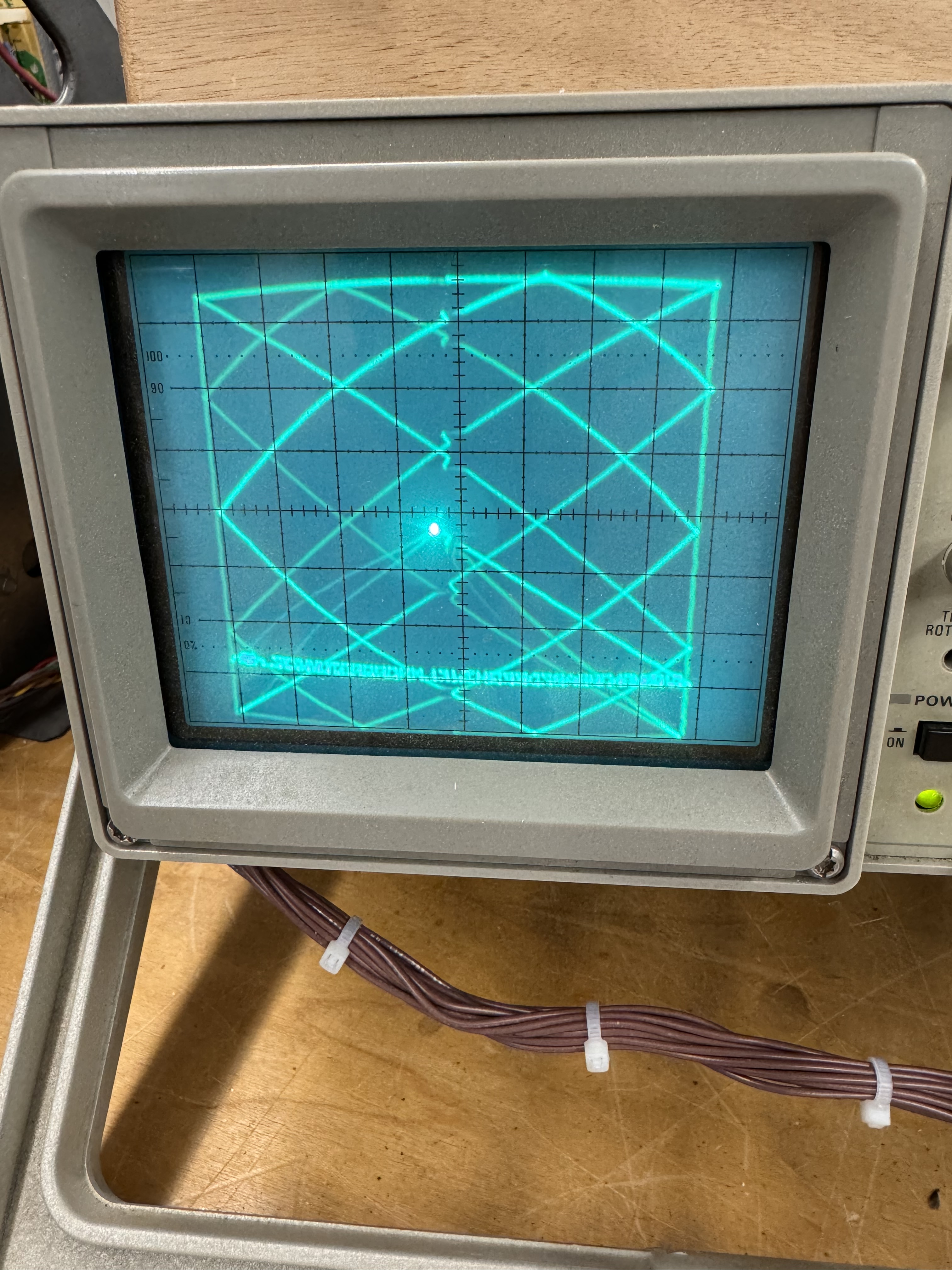
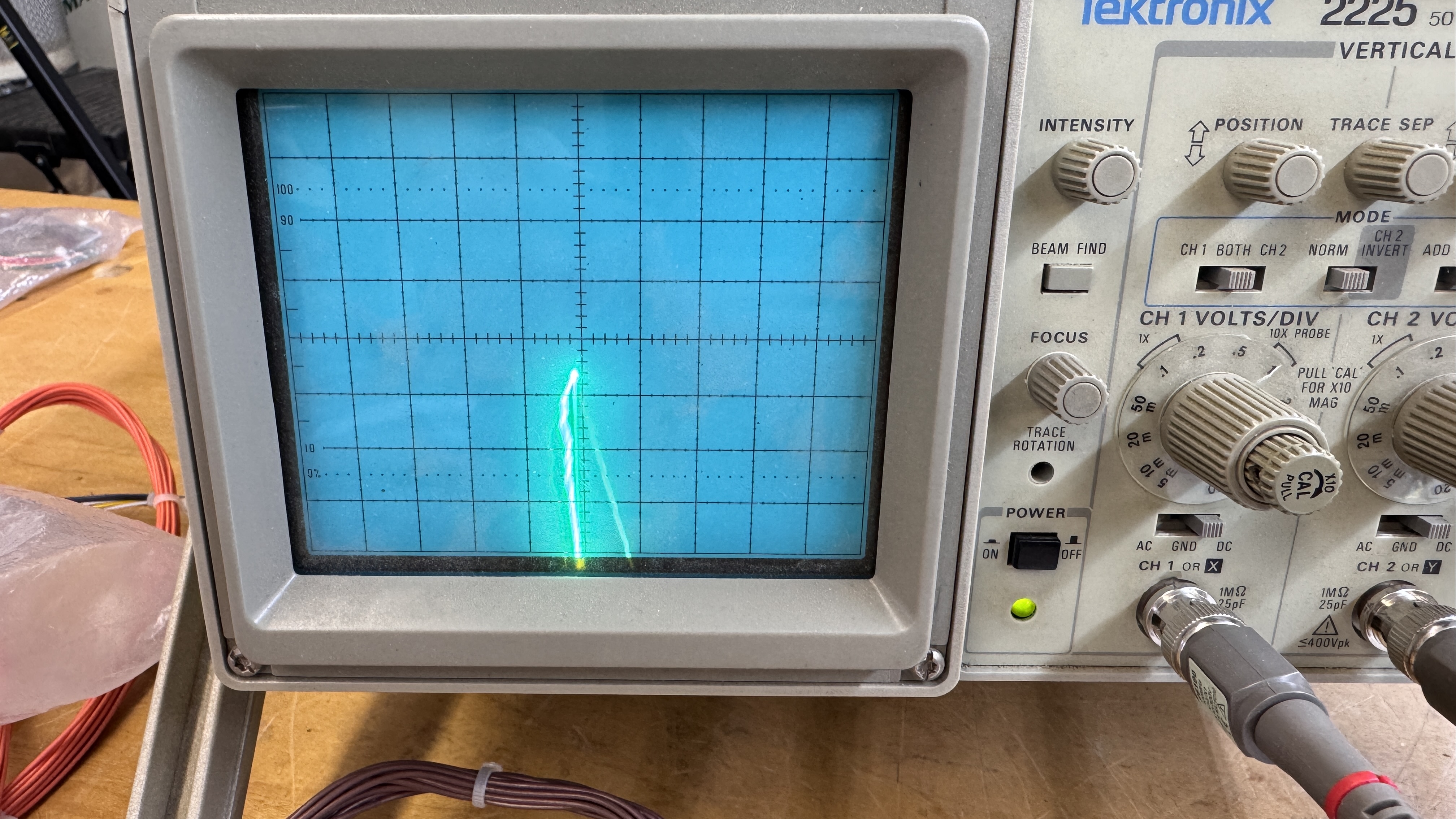
Tempest sets almost always have cold solder joints. Part of the inspection is to identify and reflow all of them. Powered on, this was the first image on the scope.

Looking at the image – it shows the x-axis working and the y-axis not going above 0v. A good place to start. Clipping to the TL082’s showed bad output too.. In this case it’s usually difficult to determine if the issue is the DAC or the TL082.. but not this time. The DAC@F10 was outputting a small voltage on pin18, it shouldn’t do that. DACs output current. Replacing the DAC got the analog section working.
From there it was immediately noticeable that there was no sound.
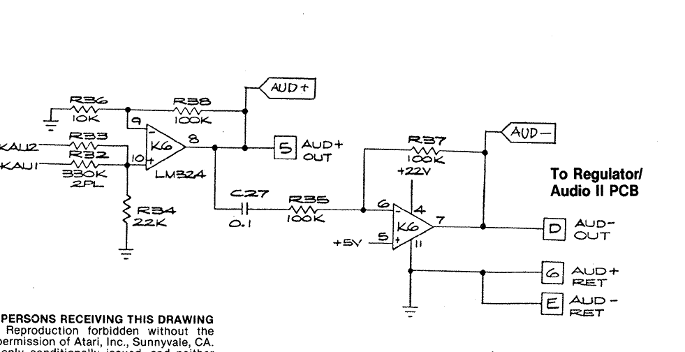
LM324@K6 on the AUX board was bad. Socketed and replaced. We now have sound! Except the bad news, one of the Pokeys was bad.. Swapped in a replacement and the board was working. During the first burn in cycle (12 hours run time).. This happened at around the 3 hour mark..
This turned out to be a failed analog switch@E11. Ran a few more hours and the other Pokey failed. Ouch! 2 bad Pokeys..
Started over on burn in cycles – this board has obviously sat for years w/o running.. I see these types of burn in failures when they have not been powered on in a long time. It has now made it through all 30+ hours of burn in testing w/o additional failures.
Board works!
Board 32– Board in for repair
This one came in with intermittent crash issues. Pressing on the board caused it to fail.. vibrations, etc.
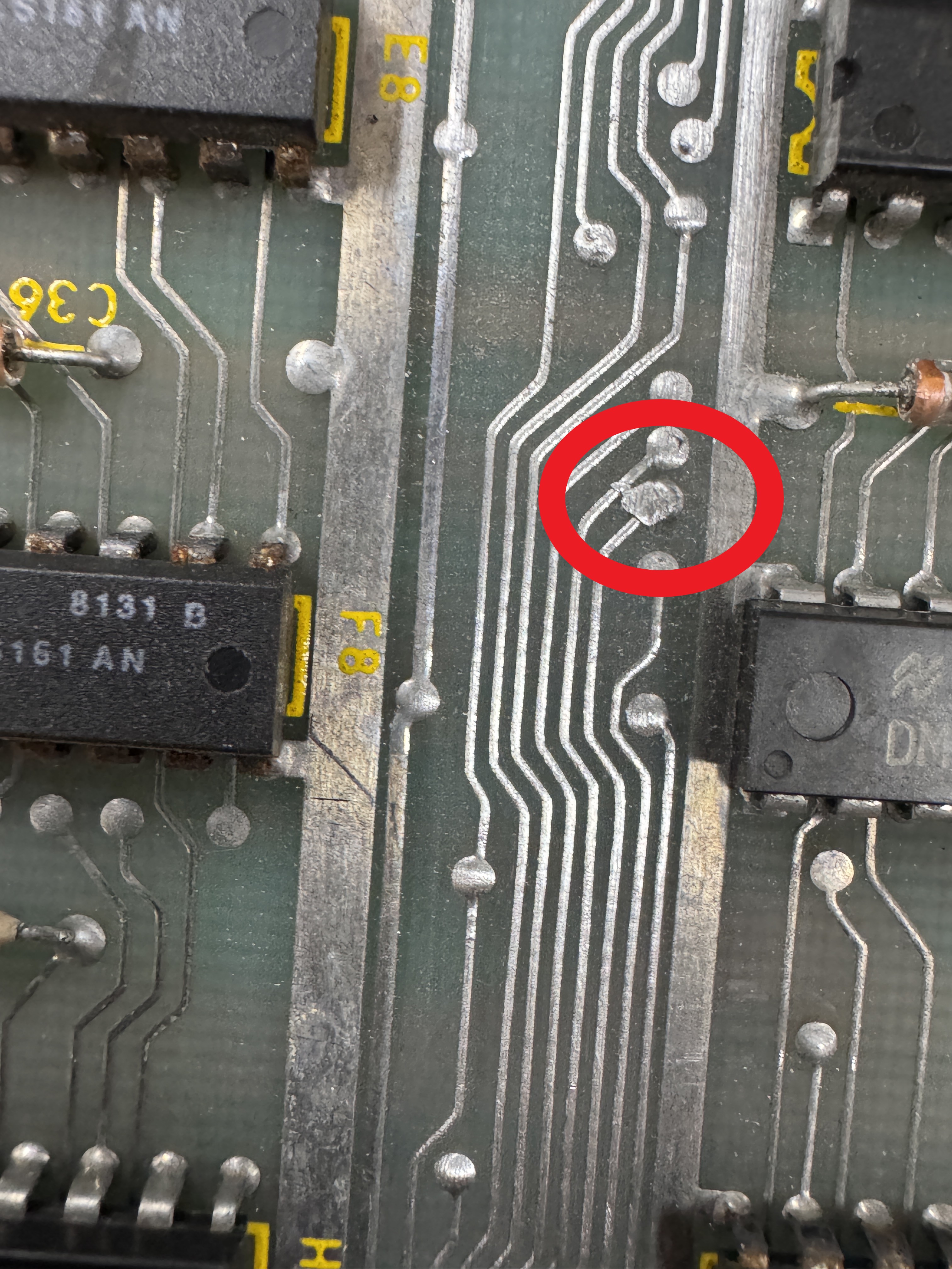
Normally with this sort of issue – I check the headers, reflow, etc. This particular board had nice dual wipe sockets and all the ram had been socketed. It took a while but during testing I could get bit 6, 7 and sometimes 4 to fail on the data lines.
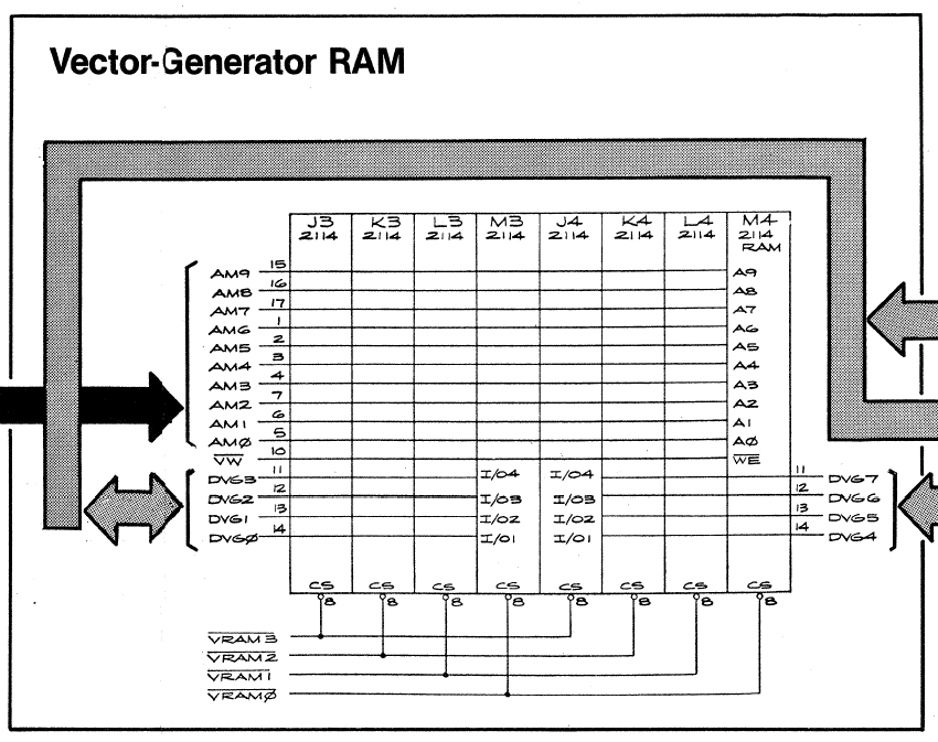
Looking at the schematic, address line 6 is on Pin1 and the RAM had all been socketed. Pin 1 is adjacent to the 5v+ rail and flexing the board caused a solder whisker to make contact. It took a while to find because it wasn’t obvious where the intermittent short was. A6 goes to a LOT of places! The RAM@M4 was the one with the short. All physical issues with RAM and addressing were resolved. However – all the socketed chips were heavily oxidized and needed to be cleaned. I could generate failures just wiggling chips in their sockets. Finally the board got a set of sealed pots to replace the standup pots.
Board works!
Board 33 – Board in for repair
Board came in reported not working. It was watchdogging when I received it.
Initial inspection showed some cold solder joints on the interconnect cable. After checking ROM, RAM and the vector generator. The board booted but was very unstable. I cleaned all of the chips making sure to remove the black tarnish lines that develop while in touch with gold sockets over 40+ years + Deoxit. This eliminates that ‘crunchy’ sound do the boards and the contact is much better.
I also replaced the plastic standoffs (they were all broken – hopefully not from shipping) and replaced all of the standup pots (one was busted)
Full 36 + hour test cycle.
Board works!
Board 34 – Board in for repair

Received a Tempest reporting graphics issues. Initial inspection and chip cleaning happened at the lake.. It had some work done in the past with a mix of adjustment pots in the analog section.
After cleaning and Dexoit, board ran but the graphics were in bad shape..
At this point I had not replaced the pots in the analog section (which I always do on boards with the the stand up analog pots).. This corrected all of the graphics issues. The last issue I’ve known existed, but had never seen in person.
Updating to R3 ROM set fixes this.. It is a function of an early deflection board and ROMs. I’m using a different bench monitor in this case.
Board works!
Board 35 – Board in for repair
Board received with reported graphics issues. Board maintenance consists of removing chips, cleaning legs and replacing the original standup pots with the sealed cermet ones – shown installed.
It also had a Tempest multi kit and ROM eliminator installed.
Here are cold solder joints – most Tempest sets have them and they always get reflowed. The DIP switch bank @N13 was also broken.. It got replaced.


Chips getting popped out and legs cleaned, legs and sockets Deoxit’d. I’ve added a third test station. This one is more or less dedicated to my automated power cycling (torture) test.. The goal is not to find out when the board breaks – it is to power cycle (30 min on, 60 min off) for a 24 hour period and see if the board works once completed. If something is going to fail – I want it to fail here. Bench space in the shop is at a premium and I have two test rigs running out there. This one allows me to keep those running and power cycle boards. It sits on top of my desk in the office. After all the repairs and testing.
Board works!
Board 36 – Board in for repair
This one came in with the board above.

No ROM and No CPU. Owner asked for a multi-kit as well as to get it working.

I replace all of these – but here is one of the reasons.. they little guys take a beating and they haven’t stood up over 40 years.
Plugging into the tester..

Had some single bit errors and full RAM errors. @P2, R4, K4 had single errors. @L4 was all 4 bits and it was corrupting @M3. Once all of this got sorted and RAM tested good..

ROM@R3 tested bad.. It was a mask ROM and had completely failed.. Replaced with a freshly burned EPROM. This got the board to a state where I could test the vector generator. It seemed to be working but the output was a mess.. Tracking down the root cause took a while because there was a dual failure with symptoms of a single failure..
Testing showed corrupted output on the Y side of the analog section. The test pattern would show, but way off the screen.. Popping a few chips out and socketing didn’t resolve the issue as it usually does. Finally I found this testing the input to the DACs
Here just the right data bits were being dragged down to keep the test pattern as expected – but off the screen.. There is a first time for everything – I had not seen this fail this way before. Finally tracked it to this..
It was shorting a couple of lines together.. The second failure that looked identical was the TL082@D/E13. It had the same ‘Y offset’ failure – just later in the circuit and was unrelated to the short. The combination of these two failures and that they were the same symptoms took a while to track down..
During the first 10 minutes of the board running on my 6100 – the whole screen shifted to the left and the monitor went into spot killer/save it self mode.. The 1495@C13 failed right before my eyes.

Here it is power cycle testing with my own version of a MultiROM eliminator. It has a push button switch to toggle between Tempest and Tempest Tubes. There is a reset button on the CPU adapter so that you can flip games and reboot without having to power off the machine.
During my final test day and checkout.. the vectors were going crazy and the AUX board was showing failed.. ughh.. I checked all of the header pins and they were 100% after the reflow. It is likely the interconnect cable pins are just slightly loose and contact with the round header pins is not secure enough – even though wiggling the cable didn’t seem to make a difference. I replaced the round headers with the beefier flat ones. They will make better contact in this case.
During testing – I noticed this. Tempest logo stair stepping. It also had an issue where the logo would “squeeze” on the left corner on occasion. Normally this is the DAC-08 in the analog section. Swapping it did nothing. There is an LS273 that feeds it. It seemed good too – but I swapped it just in case it was doing bad math (also not the issue). The root cause in this instance was C70.
It was partially shorted – reading about 40K ohms.. Should have been up in the meg area or reading open. Replacing it corrected the reference voltage into the DAC. It fixed the scaling and the pinching of the logo. Because this particular board had been so problematic – I ran it 30 hours coined up.. No resets. Should be good now.
Board works!
Board 37 – Board in for repair
Board sent in reported: locked up.. Wasn’t doing anything for the owner. When I received the board very little worked connecting to my tester. I got a couple of RAM to verify and a ROM here and there.

Next to the CPU .. there was a lot of what looked to be trace damage. I fiberglass brushed it away. The next issue was that the EPROMs went in and out of the sockets really hard and they would randomly verify. I generally do not like to just replace sockets, but it was called for here.

Here they are all cleanly removed and replaced with dual wipe sockets. This takes a while.. I also replaced all of the standup pots with sealed cermet pots as I always do. These and a CPU socket got this PCB cooperating. I could verify RAM and ROM. It appeared to be all set…
Except for this:
This glitch didn’t always happen, but tended to happen at the same place in the game at this level. I could run it for hours.. or I could power it up and have it happen within a few minutes. None of the built in tests failed.. Eventually I focused on the bit slicer chips looking for a marginal one that didn’t fail self test.. Many nights were spend watching Tempest attract mode while repairing another PCB.. It appeared swapping two of the bitslicer chips with a different brand of the same was fixing it… but it all didn’t make sense. During all of this I replaced the bitslicer sockets and 2 of the PROM sockets that looked a little suspect.. But they were not the issue either.
I started my repair checklist and the hint came when starting a 2 player game. Player 2 flipped like we were set up for a cocktail.. That should not have happened. I traced it back to the Pokey @B/C2. Pin 10 was stuck. Swapping to the other slot showed that it had developed more issues that were not there previously.
I swapped in a new Pokey and put back the original bitslicers. Ran many times and no more issues..

The Pokey is on the databus and must have been corrupting it under certain conditions. It was a very subtle failure that took a couple of weeks of bench time to find..
Board works!
Board 38 – Board in for repair
I often plug in a board that has no visual issue just to see what it does. Plugged this one in and it was stone dead. Even on the scope – nothing happend.
Connecting into my tester – RAM checked good. ROM was all over the place, I could jiggle them and sometimes they would pass and other times not.. It had the Atari gold pincher sockets which are the ones most likely to cause issues. 10% of the time I need to replace them all.. All of the ROMS were extra crunchy going into and out of the sockets.

Many times just washing the board and cleaning chip legs resolves that issue.. It did here..(mostly)
Part of all Tempest repairs – and nearly all boards with the stand up pots is replacement with sealed cermet pots
The originals are often broken and they cause the jitters. Sealed pots are much more reliable.


Plenty of cold solder joints to reflow too… Pretty easy to see.
Once back together I got all but one of the ROMs to verify..
It was an original mask ROM – There were a few areas that were the same – but most of it was wrong.. I like to compare them just to see how bad they are. This board had V1 Tempest ROMS. I erased the three that needed to be reprogramed so that this was a V3 board (217, 222, 316).
Once this all got together – I was able to get the game to boot. But it was messed up. In diag mode – It showed a bad Pokey (ouch.. expensive).. replaced it and ran it over night. Next day, board was watchdogging.. I reseated a couple of ROMs and it ran through more test cycles..
On the last test cycle day – I powered it on and the video blinked in and out a few times.. Like someone was messing with a light switch.. Then it ran fine for a couple hours.. Failures like that are sometimes difficult to narrow. I put the board on a power cycle test over night to see if I could shake out the bad chip – and I did.. The TL082@D/E12 had failed. It partially working can cause the monitor spot killer to kick in… Unfortunately (well – better it fail on my bench then back with the owner) – the other Pokey died. Replaced it..
I re-ran the power cycle test with no issues.. However – part of testing is a “physical” test.. Moving the board .. dropping it a couple inches onto the bench. etc.. The goal is that it shouldn’t ultra fragile.. Doing this caused it to cut out again.. The Atari gold pincher sockets have to go..


Removed all on the CPU board and replaced with nice dual wipes.. Ran one more over night test – no resets and no issues with physical testing.
Board works!
Board 39 – Board in for repair

Reported symptoms were graphics issues. This set has a lot of miles on it.
Stack was running – graphics issues confirmed. After checking voltages in the analog section – I checked the output on the DAC@F10 – pin 18. Here you can see voltages coming out.. we shouldn’t.. DAC was bad and replaced.
The RAM@R4 was also bad.. it had this oddball socket, I replaced the RAM and the socket.
After that – the board set had a lot of physical issues. Hot glue was used to hold things in place (that didn’t need it) in a number of places.. All of the board spacers got replaced with proper ones and the standup pots all got replaced as is standard on all of my repairs.
ROM set was updated to V3.
Board works!
Board 40 – Board in for repair
Here it is completed and during final testing on the bench. New adjustment pots in the analog section. It also got all of the standard board maintenance.
Reported symptoms were the graphics issues. During initial testing it showed a bad RAM@J3, replaced it.
From there it showed a mathbox failure. I chased it around a bit but it was clear the addressing counters LS161@D1 and C1 were not functioning properly. Early on it looked like the LS08@E4 Pin 6 was the cause as no clock pulses were being generated. Pulled it and it checked good. Next in line was the LS161@D1. Pulled it and it checked good. Last I pulled the LS161@C1.
It was bad. It was pulling down the counters from the input side of the chip. Which made it difficult to determine as the root cause. The last part is a bit of a head scratcher, had to replace all of the PROMs.. they all read blank. Not sure it the machine took a power hit.. It had not worked in over 6 months. Replaced them.
Board works!
Board 41 – Board in for repair
This one came in not working..
Clean Tempest board. But certainly had some issues. I started with normal board maintenance. This one belongs to an arcade and wanted it to be made as reliable as possible. Cleaned all the chip legs, Deoxit, etc..
Replaced all of the original pots. Two were broken or close to it.. These sealed ones are much more reliable.
Cold solder joints all through the interconnects.
Once it was up and running – it had a Mathbox error.. Turns out 2 of the PROMs on the AUX board were put in backwards. They were dead.. Once running, determined one of the Pokeys was dead. Ouch!
Replaced them all.
Board works!
