
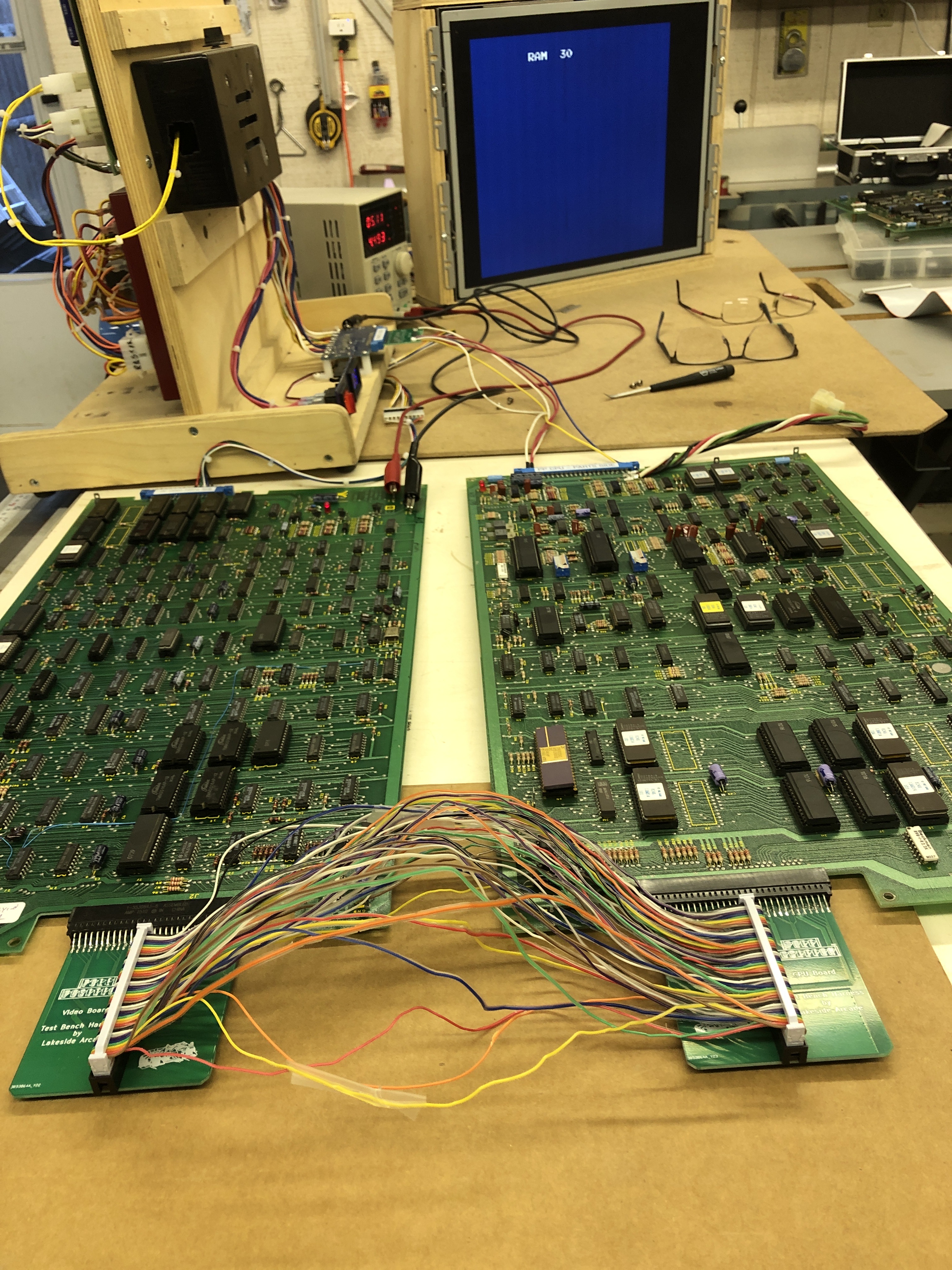
My plan had always been to work on Pole Position PCBs. I have 4 or 5 sets myself, I just never got to them. My test bench adapter was rather easy to assemble as compared to some other ones I’ve built. The video board is just 5V+ and the video signals. The CPU board is just 5V+. While getting set up for the very first time, I pulled out some of my boards and amazingly I got a fully working set. GREAT! Reference boards!
Board #1 – In for repair
Initial board cleaning took almost 3 hours. Over 50 chips removed, legs cleaned, boards washed and inspected. Sockets Deox-it, chips Tarn-X, etc. That was only the beginning….

Remaining maintenance work was to replace the existing edge repairs (they were way too thick, I measured with calipers) and repair battery damage on the CPU board. After all that maintenance, I wanted to see if the video board worked…

It’s all jury rigged together at this point, but RAM3 error – replaced ram @7H and cleared it! Video board was up and running with my CPU board. It’s obvious why there are 2 ARII’s in a Pole Position. The video board alone is pulling 4.5A.
A year ago when I decided to work on PP boards, I designed this Pole Position Bench test adapter for the interconnect so I could lay the boards flat. I never got around to testing it until now.

The first time I fired it all up it worked! Unfortunately it works ‘unreliably’ at best. Some boards it works and others it doesn’t. I get RAM errors on the bad ones. If I put the factory interconnect on – RAM errors clear. I would think at the slow speeds of 1980’s technology, timing would not be an issue. I’m not an electrical engineer.. so some of this is guesswork. But I hypothesized – maybe there is crosstalk/noise because of the ribbon cable?
As a test, I carefully separated this ribbon cable over the course of an hour…
Same CPU board, different video board. Random memory errors. bummer. Then I thought, resistance? I checked resistance point to point on the factory interconnect. It was anywhere from 0.1-0.2 ohms. On my adapter – if I checked the resistance on just the ribbon cable connections on the back of my PCB – 0.2 ohms connector to connector. (good)
Testing out to the edge connector.. i.e. including the PCB traces. Testing grounds – I still get 0.2 ohms. This is because I had wide ground traces in my design. Testing the data and address pins, I get 0.4 to 0.5 ohms end to end. My current theory is I accidentally limited current to such an extent that the boards cannot drive whatever is needed on the opposite ends. I used the default trace widths in KiCad. I’ve revised the design using wider traces to see if this will provide consistency. It would be great to be able to reliably test these boards flat on the bench. Stay tuned – I’m waiting for the new PCBs to show up..
On to the CPU board. I wanted to clean up the edge connector repairs.. I’m sure they worked, but they were extra thick. After removing the bad ones..


You can see the divot from the burned up finger. I found this UV cured resin that has worked great for lots of these types of small repairs. Filled the divot and then using a razor after it is cured, I scrape it down flush with the PCB and added copper tape. When they are all done they get coated with liquid tin to protect all the copper.
On to the battery damage..

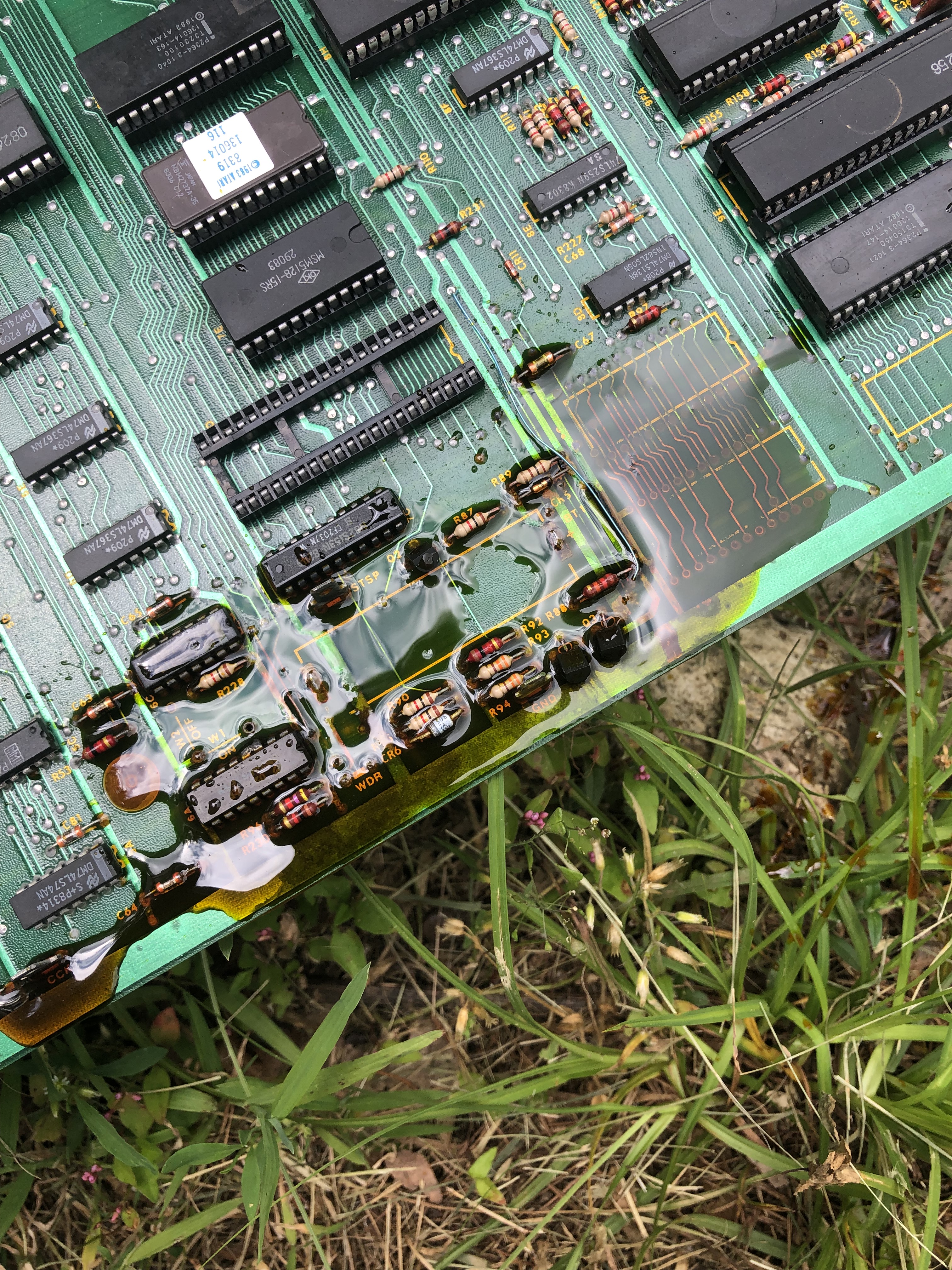

Not as bad as a couple of my other boards. But needed to be addressed. I used etchant to help with the alkaline damage front and back. There were also solder side jumpers which I removed as part of the repair (not a fan and I remove them whenever possible)
After the first time through, it had removed the surface damage, but more importantly it helps the damage below the solder mask bubble up enough to be scraped off easily. At that point it got a second application of acid to get the rest of it.

From here I used the fiberglass pen, a wire wheel and some sand paper to try to polish up the copper traces as much as possible. I also removed all the jumpers front and back and repaired the traces on the parts side. After all the cleaning and giving it a coat of liquid tin…

Not bad for my first PP board. Next one will be even nicer looking.
Finally.. on to actually repairing the CPU board!
Connected up to the CATBOX and all the video RAM tested bad.. Replaced the WDF test point which was missing so I could disable the watchdog. After a lot of poking around since this was my first PP repair – I determined the RAM was never getting write enabled. Backtracked through the circuit and found this area:

This custom is the traffic cop between the D0, D1, D2… data bus and the DB0, DB1, DB2… data bus it seems. Video RAM is all on the DBx bus. However it was never getting enabled @PIN27 SYSDBENBL. Working backwards again..

The PAL@7C Pin 15 was dead. I pulled one from one of my other boards and now all memory tests pass. It wasn’t battery damage or a broken leg.. Just that pin didn’t work. I suppose alkaline could have crept up the leg .. maybe..
My last issue was the voice cutting in and out randomly.. At first I thought it was a bad socket, nope.. These little guys were just close enough to sometimes touch and sometimes not.. Missed it on initial board inspection.

Full testing happens in my Pole Position Cabinet, however I do like to be able to test on the bench to limit the back and forth. I’ve built up a few different controllers for my test rig. The trackball controller was best suited for the task in this case.
Testing with my steering ball, gas knob and shift rocker switch!
Board Works!
Board #2 – In for repair
Technically this is the third PP I’ve worked on. The real #2 is one of my board sets. I cleaned it all up connected it up and it worked. Someone sold me a working set. I’m guessing cleaning the tarnished chips fixed it. I didn’t bother to plug it in before cleaning.
This Pole Position II set was sent in and I wanted to work on it because my personal cabinet is a PPII and I have a non-working original board set with matching serial numbers for that cab.

Between this board and the video board – cleaning all the chips, verifying all the ROM and RAM, etc. Nearly 4 hours total with cleaning up of alkaline damage.


This one as not as bad as most. I cleaned up the damage with acid, fiberglass brushed it all down to copper and then used liquid tin to recoat it. It tends to be a little blotchy at times.
Right out of the gates – ROM 182 and ROM 106 were bad. Many of the CPU board chips had broken legs and were rotted.
I first plugged into the Z80 CPU with the FPGA Catbox. I was not able to see RAM/ROM. Same as the first board I worked on, the PAL@7C was not working correctly. I socketed it and replaced with a GAL16V8. Now I can see all the RAM and ROM. Visible to the Z80.
I had put all the customs and CPU’s in that came with the board (that had legs) and started working on it.. After a while I realized this was a bad idea. I stripped the board of all this stuff and put all known working customs and CPU’s in and started over. New rule on PP – Just do this.
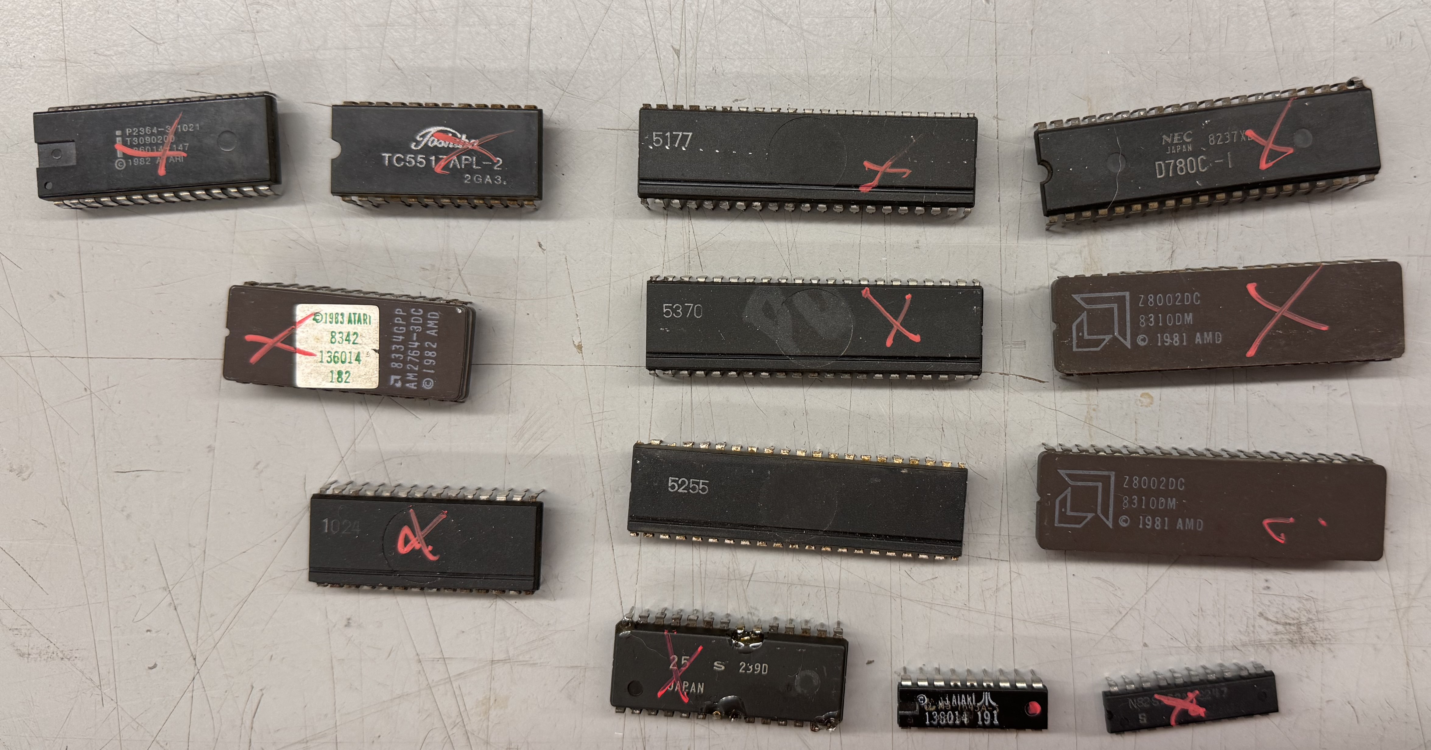
Here are all of the socketed chips that are dead, rotted or otherwise partially working. All 3 CPU’s, All 3 big customs, RAM, couple of ROMs, PAL and the color prom from the video board.
Once I got all the good/bad separated, things went a little better. All of the sounds 1-16 were messed up. They had a beepy quality to them. I spent a little time poking around until I came across the 74LS283@10F

Replacing this restored the sounds and brought forward a new issue. Many of the sounds began or ended with a popping noise. More poking around and I found the CD4066 analog switch @10L had a bad pin 8. Replaced it and cleared up some of the popping noises. What was nice is that it tested bad in my cheap Chinese chip tester. Still had popping sounds and distortion and I found a bad pin on CD4066@11L – it tested bad and helped clear some of that up.
Now it seemed the tire sound was distorted and it faded in and out sorta.. Since I had 2 bad CD4066’s I replaced the other 3 in this area because they all had the same date code, but it made no difference. I stepped to sound 17 in the DIAG screen and determine the waveform of Pin3, CD4051@11F was different than that of a working board. Had to ‘borrow’ a chip – replaced it and proper tire sound restored.
During all of this I tried to save the original IC-25 custom. Spent time replacing chip legs, etc. All for nothing – it was dead. I’d tried using the ROM workarounds, but they were not cooperating and the info out there was a bit confusing. @TimePiloteer on KLOV to the rescue.
There are two ways to replace IC-25@4K. The two ROM replacement or the three ROM replacement. I opted for the 4K Two ROM set
Burning new 2764’s with the 176-V3.3L, 177-V3.4L images and using the ROMs at those locations will effectively replace IC-25@4K. Leave the @4K ROM slot open. I did fight with these a bit and determined the Z8000 CPU’s are particularly sensitive to the EPROMS. I burned these at the same speed as the 2764’s I replaced @9C and 12E. Those are addressed by the Z80. They work fine. @3L, @4L are addressed by the Z8000 and they were not working. @TimePiloteer told me to do a total of 6 writes on the GQ-4×4 to saturate the 2764 EPROMS. It worked. Big win on this!
Last item was the checkerboard on the track edge was Red/Green vs. Red/White. Color Prom 191@4L on the video board was also bad. Hopefully that was the last of it….
It wasn’t.. I was doing a few final checks and then cleaned all of the flux from the back of the board. Connected it all back up, board would not boot. Seriously?! Checked for loose chips, etc.. nothing.
Plugged back into Catbox and it was not reading RAM@7E. Tracing signals the chip enable CMOSRAMCS was being dragged down for some reason.


Q3 was showing an emitter-collector short. I pulled it out and the short was still there (20 ohms). I traced it back to this guy (C67) who must have been in the process of failing. It wasn’t in the alkaline damage.. Replaced C67.
Board works! (again)
