
I got a request to repair an original Pong from a repeat customer. I said I’d take a look – but wasn’t 100% sure about it. It would be my ~first bronze age repair and I knew nothing about the PCB.
This first writeup is going to be a little different than usual. I normally do a repair log and try to show my thought process and work through issues – after working on this Pong board – I wish everyone who is somewhat self taught in arcade PCB repair got the chance to work on one and see how the designers were quite brilliant back in 1970-1972 to create this iconic game. There may be a bit more color commentary that usual. Pong has been written about it depth many times, this is my version of that from an non-electrical engineers POV.
Pong has no CPU, no RAM and no ROM. It is essentially just a bunch of logic chips that together put a display on a BW TV tube and you control with 2 potentiometers and a coin switch. No data busses or PROMs or tri-state chips. Maybe this is a bad analogy – but it reminds me of the brilliance of the electro-mechanical pinball machines. Just relays, switches and motors to create different machine states.
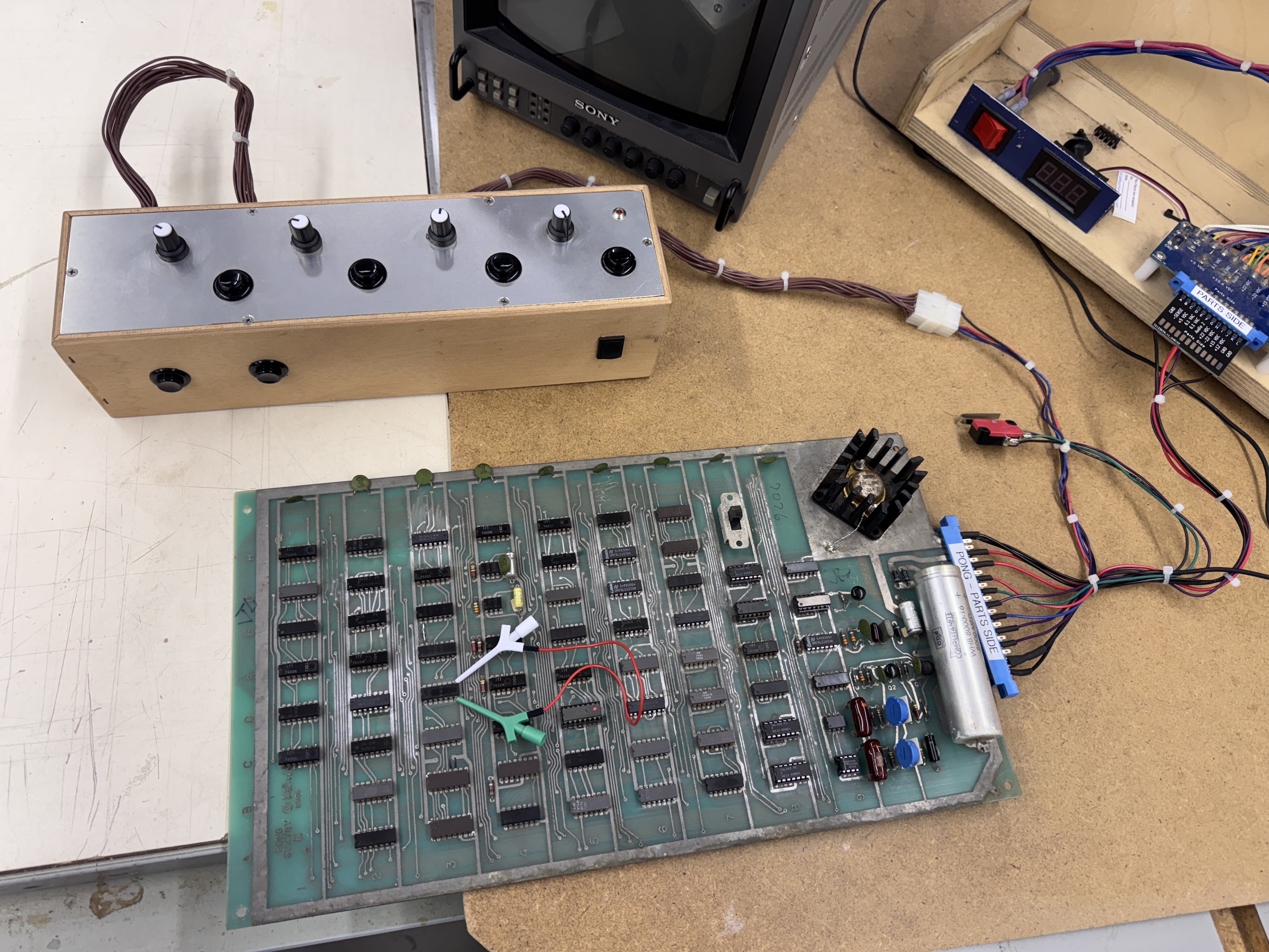
Here is the original Atari Pong with my bench adapter for my repair rig.. When I make adapters, I leave all of the heat shrink tubing floating on the wires and do not cable tie them until I know they are 100% debugged. Once I know it is working as intended I heat shrink the wire ends on the edge connector and cable tie to make them clean. Many times I have had to move or add connections and after cutting off heat shrink tubing a few times… I’ve learned. Wait until it is done-done. Also pictured is my custom bench controller for Warlords. All of my bench controllers have been useful for multiple game titles except this one. Warlords controller has been a single tasker up until now. I used the two outer pots for the paddles. Normally it would also be used to add a credit – but Pong needs an actual switch that toggles back and forth from Open / Normally closed (more on this later). I had a micro switch available and it is now a permanent part of the bench adapter.
While working thought the many Many MANY issues this board had – I had printed a copy of the schematics from an original scan which is cluttered and barely legible.
I found AtariHQ and a completely redrawn set of schematics by Dan Boris, owner of the site. Big thanks to Dan and this work done years ago that made working through the board much easier. I’ll use clips from these easy to understand schematics. While Pong wasn’t technically the first video game, it was the one that helped establish the video game industry. There are a couple of errors in his schematics which I outline below.
** On this first board I did my best to document the repair in order.. If anything is off a bit, it’s because I can’t read my own writing! But I’m pretty sure I’m 98% accurate here. There was a lot going on**
Board #1 – Pong
Pong put up an epic battle. I’m certain this board has not seen power in 40 years or so. I was told it spent a lot of time under a tarp and the original cabinet is going to have to be reproduced. The parts side of the board is very old and worn looking.


It was worse than this looks and still the board looks old..


The solder side looks almost new by comparison. First thing I did once I powered it up was to check for video out – it was dead as expected. I did check for clock and I actually had some!

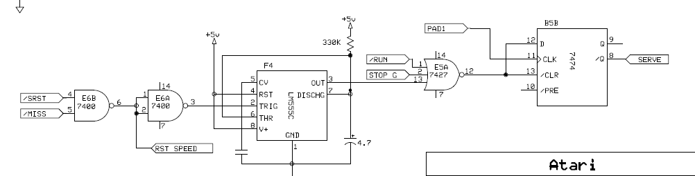
Here is the clock circuit.. Pretty simple as it should be. This part of the circuit was actually working.
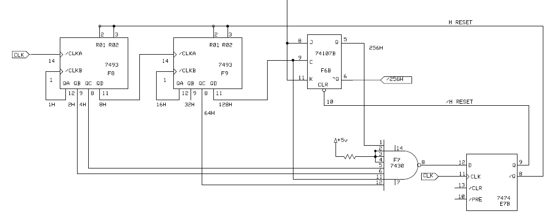
First up was 7493@F8 Pin 11 had no output. Replaced it.
Down the line 74107@F6 had floating outputs pin 5,6. Replaced it.
7474@E7 no outputs pin 8,9. Replace it.
/H RESET is now outputting a familiar 15.729khz horizontal sync frequency!
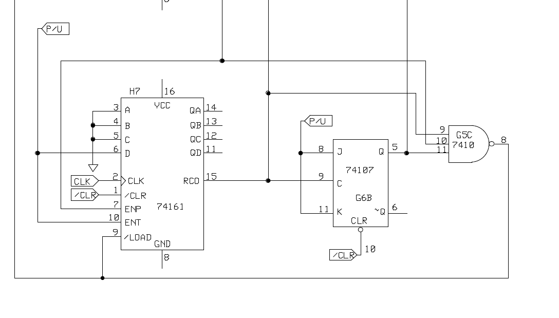
Moving over to the vertical sync section….
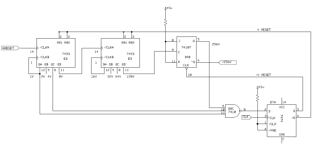
Followed the clock through these counters – 74107@D9 Pin 5, 6 had floating outputs. Replaced it and eliminated the floating outputs.

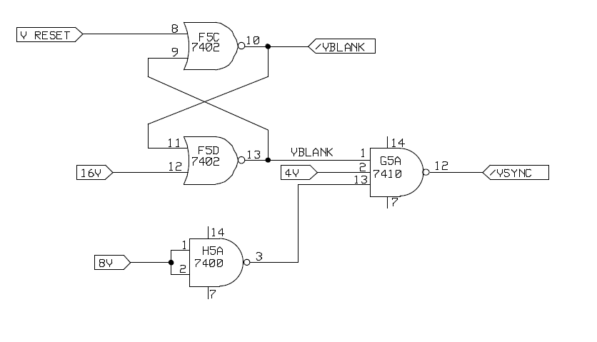
Last was 7410@G5 – no output on pin 12. Replaced it and I was getting 60hz vertical sync at /VSYNC – nice!
Finally a blank screen! After replacing 5 chips… It was going to be a long repair.
Here is where some of the simplicity and brilliance of this comes in..
PAD1 = left paddle
PAD2 = right paddle
NET = the net
/HVID and /VVID = the ball
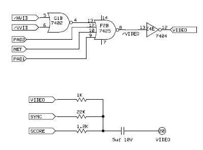
They all get combined and create the signals needed to output the Paddles, Net and Ball into VIDEO.
Next they get combined with the SYNC and SCOREs for composite output to the monitor/TV. So much easier to see how it is done here vs. more complex games.

This is the circuit that creates the Net. Not much here so I figured it was a good place to start. It uses the horizontal and vertical clocks along with the 4V pulse to create a (off)centered dotted line. At the end I’ll post a link to a 106 page document that breaks down the entire board in very fine details. It is very well written and gets into signal timing, etc. I understand a fair amount of it and other parts I’ll have to read a few more times.. The NET on the original Pong, as it turns out, is a little off center. Other variants had fixed this issue.
In my case – the 7427@G2 had no output on Pin 6 – replacing it provided the Net!
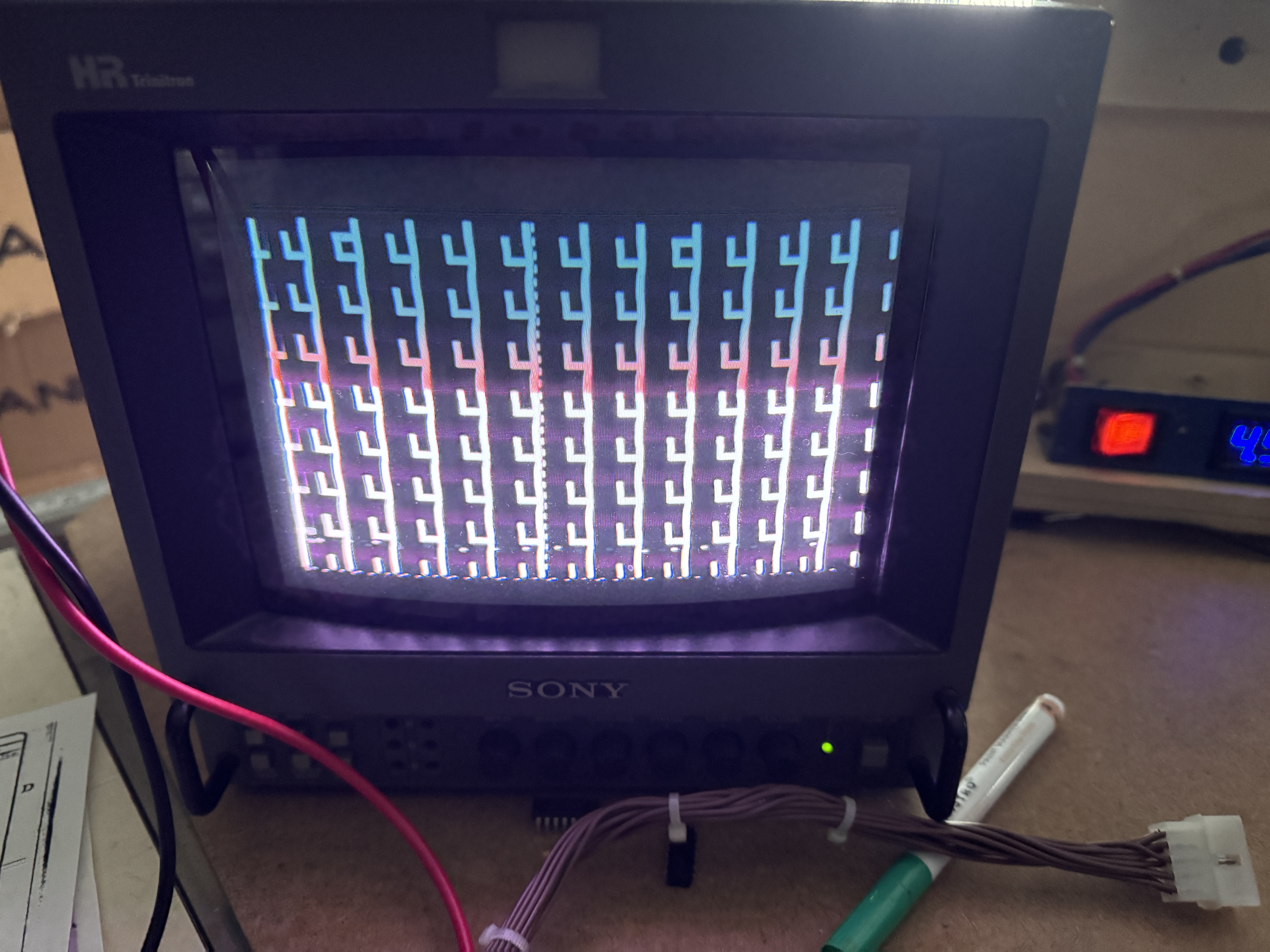
My first bit of pong is appearing! It was around now where I went from OMG I’m going to have to replace every 3rd chip on this board to .. This is a very good education in following TTL logic and seeing how all the chips work together which we take for granted today – but in 1972 was pretty genius IMHO. The long lines are some component of the paddle outputs..
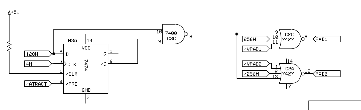
That same 7427 that fixed the net is used here in the paddle circuit – so yay! That is why the paddles appeared when I got the NET working. While in the paddle circuit, I noticed /ATTRACT Pin4@H3 was floating.. I followed that backward below.
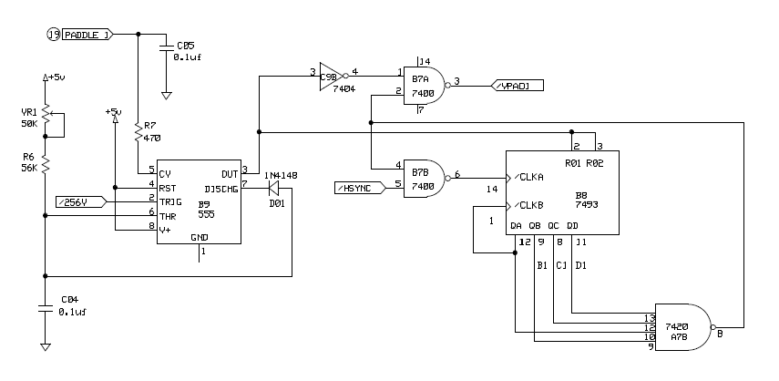
I wanted to see if I could get the paddles to be right sized and moving. During the many sessions with this board – Paddle2 disappeared.
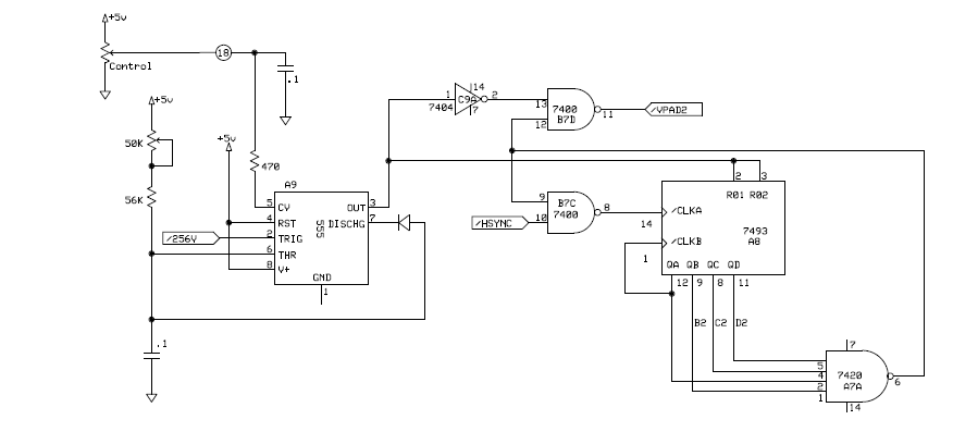
Poking around the Paddle2 circuit – The output of 555@A9 Pin 3 was dead. Replacing it brought back Paddle2. I replaced the 555N with a 555P – this will be relevant later in the story..

Back to the floating /ATTRACT. 7402@D2 Pin1 was the cause. Replaced it and that brought me this..
I call it the coat hook screen – But what it really is .. is parts of the score counts being repeated over and over. While probing the board and finding dead pins..
7400@E6 Pin6 was floating – replaced it. No changes. This is part of the game control circuits and controls the ball speed. (I believe. I didn’t spend any time here after replacing @E6). I was trying to get the ball visible and moving at this point. With the schematics broken up into these smaller units, it’s easy to see how they all work and then meet each other later in the design.
Here is part of the horizontal ball counter circuit. The 74107@G6 had a dead output, replaced it.
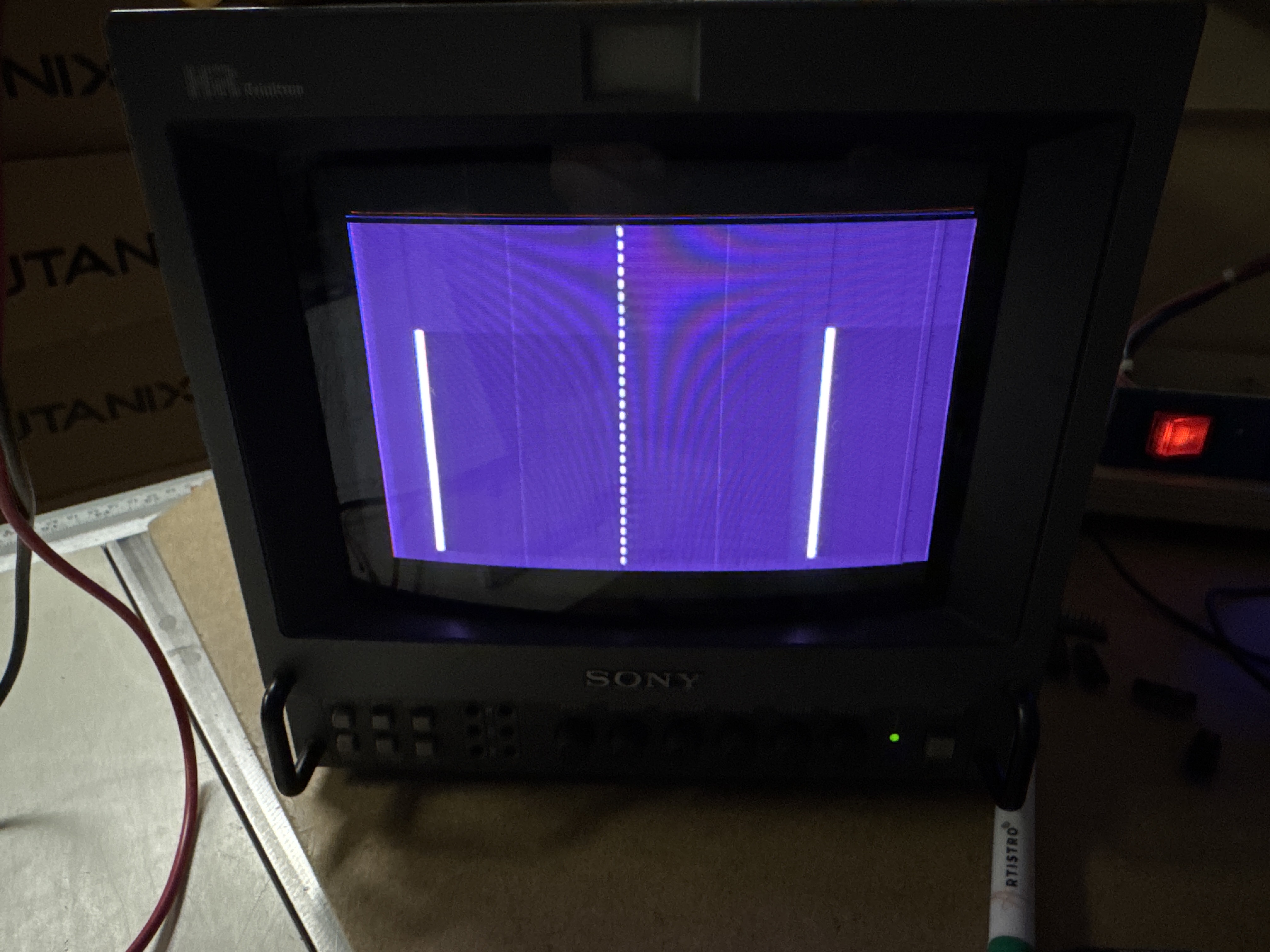
Look close! A have a ball on the screen.. It was very exciting. There was a ball and it moved in attract mode. Hidden in there were the long vertical paddles.
I had been going back and forth between trying to fix the paddles, get the ball moving and get the scores to display in the correct spot vs. the ‘coat hook screen’

I’m calling this the windowing circuit – it enables the 7448 when it should be displaying the score in the top corners. 7425@F2 Pin6 was always high. Replacing it got the enable working properly, but didn’t really fix the coat hook screen at this time. I disabled the coat hook screen with jumpers (grounding the SCORE signal) and went back to the paddles.
Here is the PADDLE1 circuit. The 7493@B8 had a bad output on Pin8.

Replacing it changed it from a long vertical paddles to a correct width PADDLE1 and not sure when it happened but something failed on the PADDLE2 side and made this wide vertical PADDLE2. Replacing the 7493@A8 corrected this issue.

Finally two normal height paddles on the Y axis.. Still too wide on the X axis.

This is the output end of the PADDLE circuit. 7474@H3 – no outputs Pin 5/6 – replaced and now there are no paddles. Pulling /ATTRACT high shows them correctly however. I had clipped another test lead here to get them to display for now. I forget what eventually corrected this.. I think I was still figuring out the coin circuit (bad notes on this part). Somewhere mixed in here there was a trace repair (surprisingly the only messed up trace on the entire board) going to 7474@H3 Pin2. which was likely the cause of the wide paddle issue. It was intermittent.
Stopped here and corrected some wiring issues on my bench adapter to my controller. I made a few connections late at night it seems.. It’s 100% now. Bench adapter is now ready for the next Pong repair. Most importantly, I was able to control the paddles.
Current Status:
– Vertical and horizontal sync restored
– Net displayed
– Ball able to move
– Paddles both the proper size and working
– Scores messed up
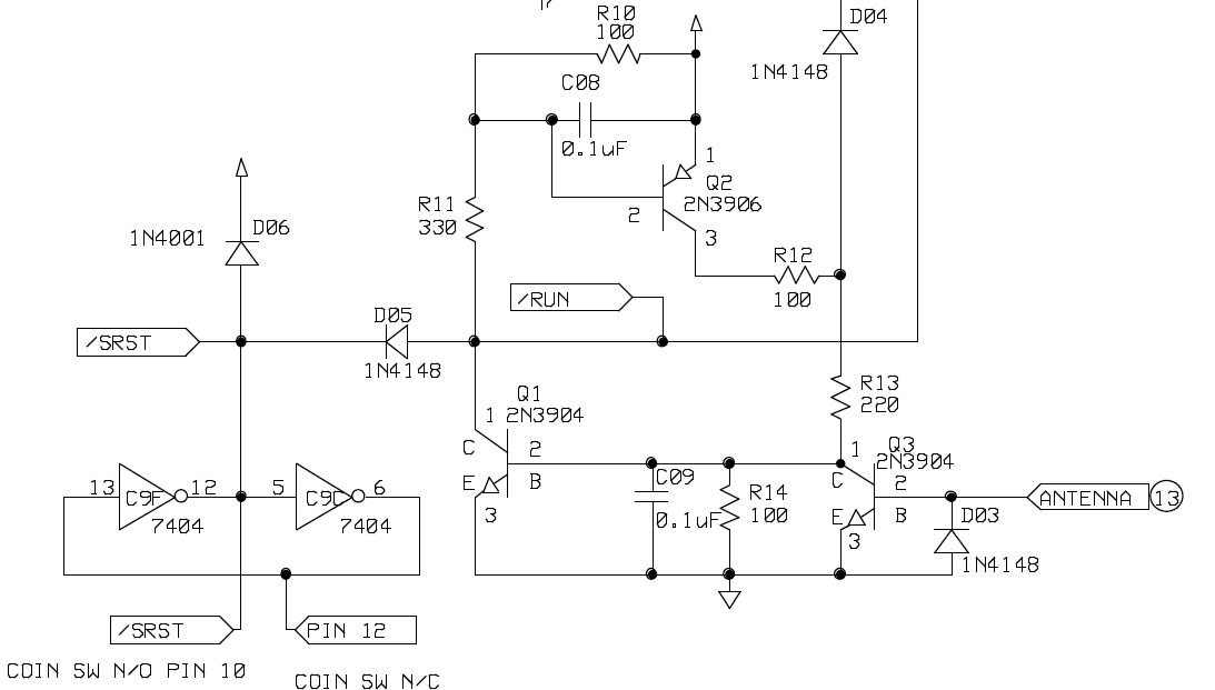
The COIN N/O, N/C switch is required. Pretty much every game I repair can use just a standard push button to add a credit. What was happening is when you add a credit – normally you just ground that side of the circuit. On Pong, the screen just went blank like I killed it?! After looking a while – I decided to ground the N/C side and the image came back. So both sides of this circuit are used to resetting different sections of the game. I added microswitch directly to my harness adapter.
Right around now is when I had found the 106 page Pong Analysis by Dr. Holden I didn’t read through it word for word yet. But it is as about in depth as you can get and did help me with a couple of items.

Here is where the actual scores are converted to signals to be displayed. The score segments are driven (earlier in the circuit) by a 7448 that was used to drive actual 7 segment LEDs back in the day. You can see the score segments in the lower right corner. They took those outputs, mapped them into the vertical and horizontal counters and created the same 7 segments on the TV screen – seems simple by todays standards – but in 1972.. I’m pretty sure this was cutting edge. In my case – I had my coat hook screen which was in the way.. I clipped a jumper to 7430@D3 Pin7 to Pin8 and blanked the scores so I could work on other things most of the time.
I had determined that the ‘Coat Hook’ screen was caused by a failed 7448@C5. But I didn’t have any and ordered some. The next day I decided I had to have something in the shop.. I Google searched on the 7448 and they were used on some pinball PCBs (makes perfect sense) I’d got a bunch of old Gottlieb PCBs from a buddy and started looking.. On one of them were 2 x 7448’s.. Perfect!
Plugged it into a waiting socket..

Finally! Scores in the right spot, even though the segments were messed up, I could now start fixing the score circuit.

Here are where the scores are counted. The 7490’s count 0-9 and the 74107 turns on the 10’s column. The 7490@D7 Pin9 was floating. Replacing it got Player2 score working..
So I set it up to count. 0, 1, 2, 3, 0, 1, 2, 3, 8, 9, 10, 11 Game ends.. Hey.. it counted! Clearly 1 bit was bad someplace. Traced the counting issue back to 74LS153@D6.

Both the C and D outputs were dead. Replacing it got the Player2 counting 0-11 (and 15 when switched to do so).
Note: While working in this – there are errors on this schematic that seem to be transcribed incorrectly. On the 7448 – the A, B, C, D connections should be:
A – Pin 7
B – Pin 1
C – Pin 2
D – Pin 6
Player1 I could not get to count. The missed paddle and hit on the wall was not registering a count. The 74LS153@C6 needed to be replaced as well. Again, some bad note taking here.. So the replacement order may be off a bit here.
The 7402@F5 Pin4 (Illustration before the one above) was not triggering a count and clocking the 7490@C7. Replacing it got Player1 counting!


Here is the end of a game. I have a few remaining issues. One is that on power up. Player2 does not set to ZERO. There is no reset pulse to clear the counter (that I can tell) and the difference between Player2 and Player1 is that P2 has a 74LS90@D7 vs. a 7490. I’ve used LS chips pretty much on every replaced chip.. I’ve ordered a 7490 to see if it matters. Once you add a credit, the scores all work as expected. Just power up is where Player2 starts with a non-number.
I had replaced the 555 chip in the paddle circuit for Player2. That paddle was wrapping around on both sides of the screen by a lot! It was not playable. After reading though the Dr. Holden document, he stated that the 555 needed to be replaced with a 555N or it would not work correctly. I had used a 555P. Fortunately, I had a 555N. Problem solved!
Last item is more of a MOD.. In the original Pong, the paddles never touched the top and bottom of the screen. In my case there is too much space and you can’t adjust it out. It is possible to start a game and have it serve the ball in the gap…. Producing a 0 – 11 score.. you lose. There is a mod where you add a diode in series with the existing diode at the 555 timers for the paddles and it changes their range just enough to go off the top and bottom edges of the screen. I did this and now there is no gap a ball can escape through.
At this point, the 7490 arrived and I replaced the 74LS90@D7 – It fixed the power on scoring issue, perfect! Now to start testing..
After an overnight burn in.. The ball died.. If you power on.. you see it zoom across the screen and that’s it.. This board has been on for hours and hours. I was a bit surprised..
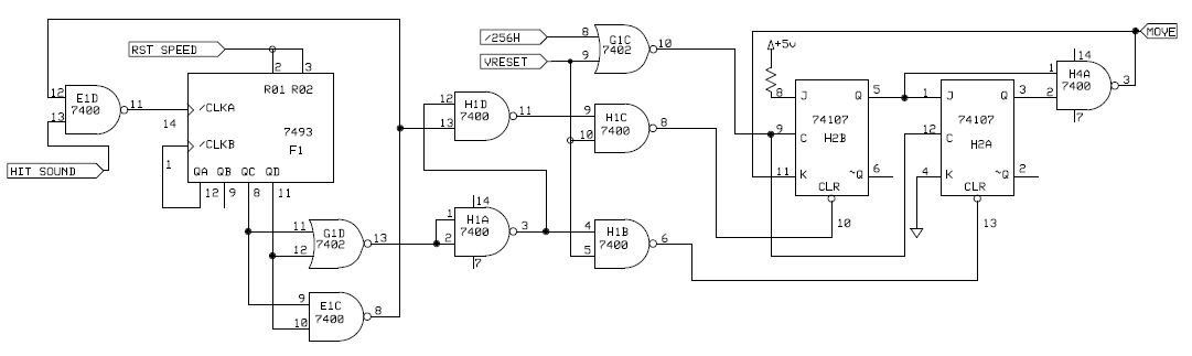
Here is the horizonal ball movement circuit. 7400@H4 Pin3 was stuck. Replacing it got the ball back – however it was perfectly stationary.. baby steps I guess. Probing around took a bit to find the next issue. On 7400@H1 Pin3, there was signal coming out. The issue was there were no inputs.. It appears internally pin5 got shorted to pin3. Up until now, almost all of the chip failures where floating pins or stuck pins or ugly signals – this one was just doing bad math (as I call it).. Ball is now moving again – but it now gets stuck in the vertical blanking area at the bottom of the screen and does not seem to have vertical counting ability (no diagonal movement)..
While looking for that issue – I realized that the ball never made sound when it hit the top or the bottom of the screen (bouncing off the walls…)

Here is the part of the sound circuit where it registers the hit – 7400@C3 Pin6 was not able to be pulled to ground.. Replacing it got the sound for the wall going. Now when the ball gets stuck in VBLANK at the bottom of the screen.. it creates a rapid ‘ball hitting the wall’ sound.. Around now is when I set this aside for a while.. I had to catch up on other repairs and I’m already well into volunteer work hours on it.. If this were a clone.. I would likely have stopped or let the owner know that this may not be worth it, some may think it wasn’t worth it at all.. Pong is not the most exciting game. But I do like preserving little parts of history when I can.. I pressed on after shelving it for a bit..

Here is the page from the schematics I focused on to try and figure out why the ball was hitting a paddle and then immediately getting trapped below the bottom edge of the screen past the lower vertical sync edge.. I probed and checked everything over and over.. and it all seemed ok. I overlooked a single clue.. The 74107@H2 – Pin 4 should have had the VVID signal.. in my case it was grounded.. even the /HIT (seemed to) work.. Now is when I put the Pong Analysis by Dr. Holden into ChatGPT looking for a bit of help.. As I asked it for input on why the ball was trapped.. It kept referring the the JK flipflop @A2.. (not H2) .. I beeped it out and determined this schematic was incorrect… grrr..
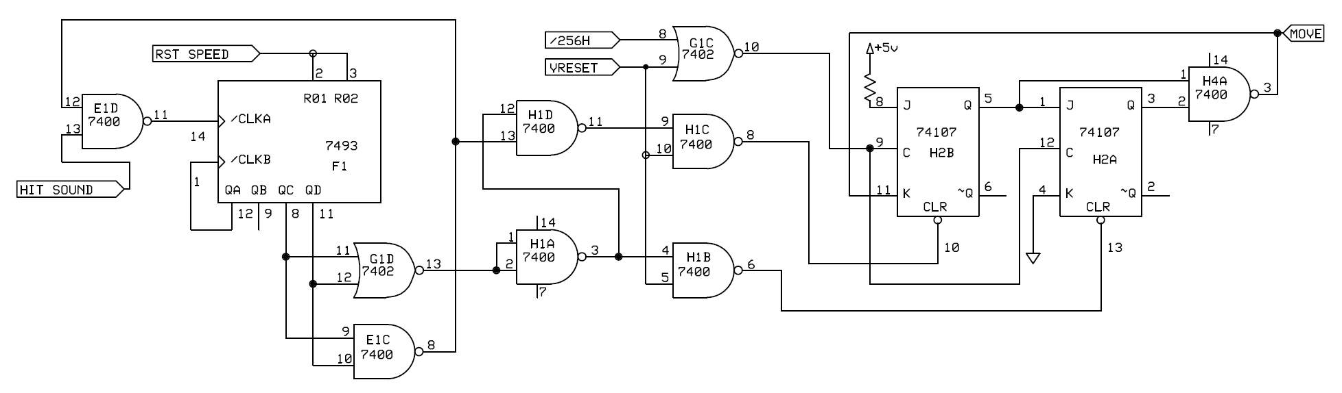
The @H2 74107 had signals and outputs all working fine. Even @Pin13 was toggling with the hit.. (at least it seemed that way – again.. Pin 4 was the clue.. and look… there it is tied to ground..
Replacing the 74107@A2!!! corrected the ball trapped below the sync signal. Finally!

While writing this up.. I found a corrected version of the schematic.. (where were you when I needed you).. The original blurry schematic was correct – I just stopped referring to it since these ones were easier to work with (until they weren’t).
This post on KLOV is about a Pong Project and the V1.3 Schematics are HERE – What’s interesting is they are identical to the Dan Boris ones except for the fix (that I can tell – but the KLOV user I don’t believe is Dan)
The last item that also took a while to figure out was this:
- In attract mode – the ball would only travel horizontally – no vertical movement
- You could enter game mode – and play a full game.
- Once the game went to attract – back to horizontal motion only
Attract mode should have the ball moving diagonally around the screen. Obviously it is more interesting than a ball just moving left and right.
I chased this one for a long time too and spent it looking at the same circuit above (and verified there were no other schematic issues. The Dr. Holden document kept talking about loading counters etc.. I just wasn’t getting it – I could even trick the circuit by pulling up the /CLR signal and powering on. Attract mode had a diagonal moving ball. I tried tricking things a few different ways and wasn’t seeing it. Finally I started removing chips one at a time and testing them out of circuit. Eventually it lead me to the 7474@B5
(I’m 90% sure it was this one.. there was another partially working 7474 that I may have mixed it with..) The part I wasn’t really understanding is the 7474 is being used to store a single bit of data.. ex: The preset counts to create the vertical ball. I’m not an electrical engineer – If this were RAM and code executing it would have made more sense to me. That said – it makes perfect sense now.. the chip was working correctly in game mode, but it wasn’t working when it was getting loaded with a starting value.. which created the bits into the counter that adds the vertical component to the ball movement in attract mode (think state machine… think state machine I need to tell myself)..
Diagonal ball movement issue in attract mode solved.

All (most?) of the chips replaced ~30 ICs.. There are a few that got replaced because I pulled originals and didn’t ‘trust’ them even though they seemed to be OK. ex: 9316 counters are supposed to be the same as 74LS161’s – my tester showed some failed tests (as 161’s) – but the 2 in question failed identically. Which tells me they are likely ok – just the tests need to me modified for 9316’s.
This repair was very interesting because it was a good test of debugging TTL logic and you got to see how the logic translates to video on the screen. If there was a course on arcade PCB repair, this should be part of the 101 class that builds the foundation for future repairs in my opinion. Later courses would introduce ROM, RAM, CPUs, state machines, etc.. I know I don’t know every little detail of how this works.. But I can see how truly clever it all was back in the day.
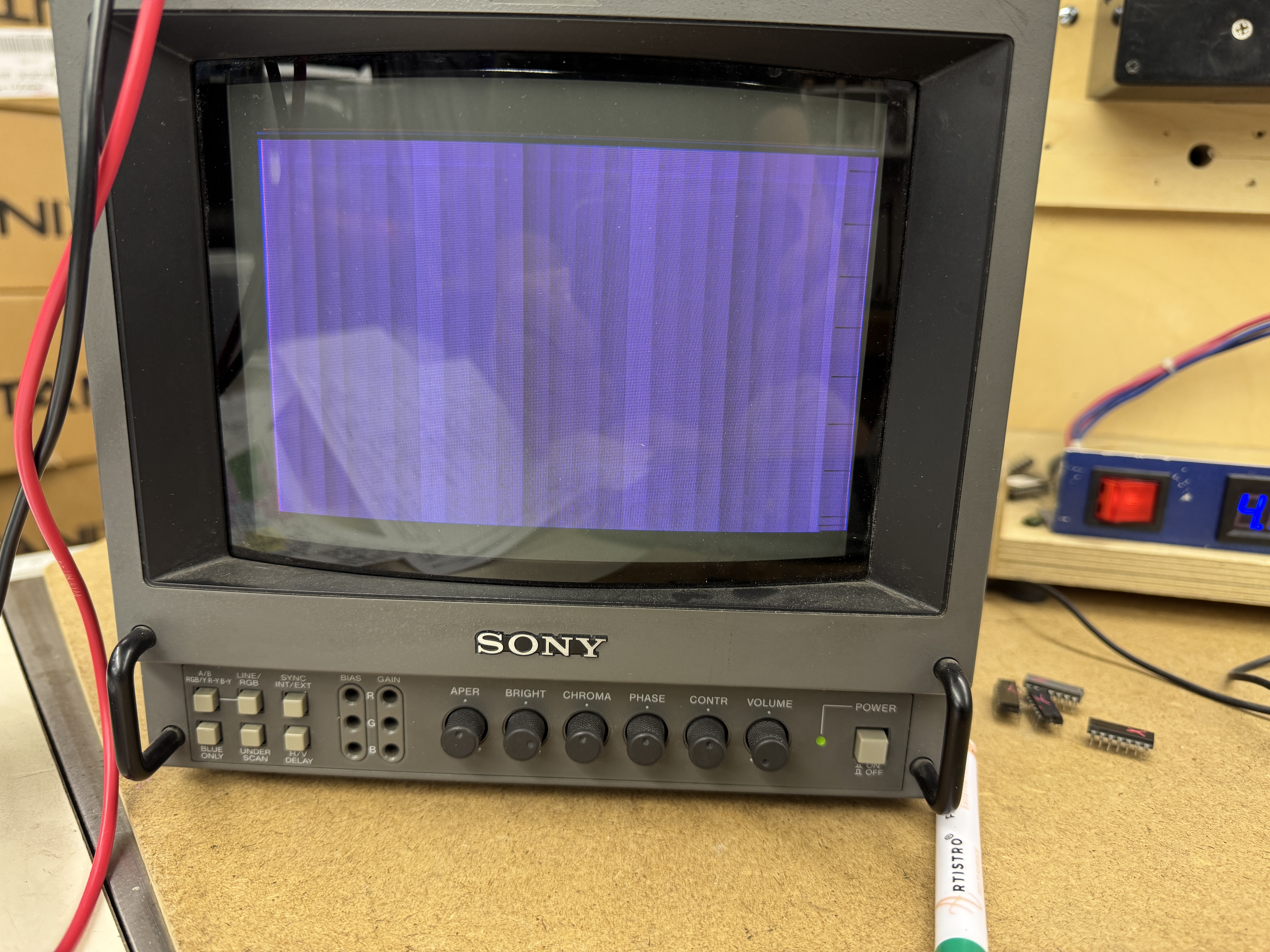
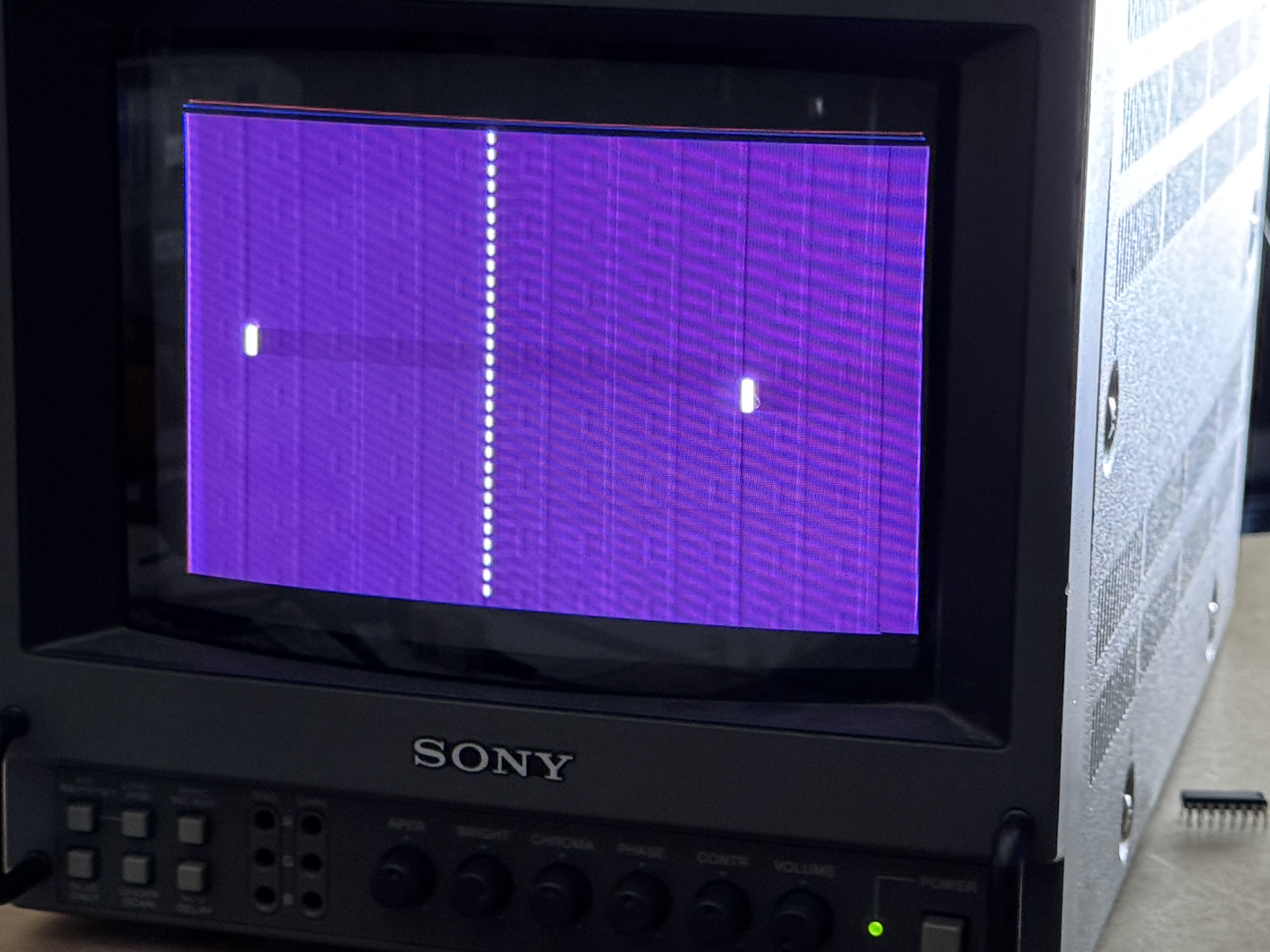
Here it is. I’m playing myself.. so not the best of action.. The little edge blips on the screen I initially thought were a game logic issue – Luckily I had the Pong clone below and it acts identically. The issue must be an adjustment in the monitor.. My PVM is a little wonky.. I couldn’t do anything about it..
Board works! (finally)
Board #2 – Computer Space Ball
A buddy who does a lot of work for collectors and arcades sent this a while back

This a near 1:1 Pong Clone. The major difference is that it is powered externally vs. Pong where it creates its own 5V via a regulator. It did cause me to modify my test adapter a bit to work with both boards. It’s actually a cleaner setup now.. I can test Pong using AC and then swap a couple connections and power with my standard 5V rig..
The other differences were 3 connections
- Coin – Jump pins 10 and 11
- Coin – Jump pins 12 and 13
- Paddle #2 – Jump pins 18 and 19
The good news is there are no conflicts between Pong and Computer Space Ball for these connections. Once I powered up the board – there was nearly nothing going on.. I started at the clock.

Probing with the scope showed I was getting 60Mhz (or so) from the crystal, really? I had to check a few different ways – but I removed it and replaced with the correct one.. Got a perfect 7.159Mhz CLK.. But still no image on the screen.. From here I probed through the sync chains and found the 7493@9F was not working..

Replacing it got sync signals and a screen image.. I was worried I’d get into replacing every third chip again.. I missed getting a pic, but the only thing that seemed wrong was the top segment of the scores was missing..
Probing through the circuit – the scoreA signal was not triggering.. a is the top segment of the Score. Replacing the 7427 corrected the issue.

This one obviously had much less wrong with it.. It would have taken a bit longer if I had not spend time on Board 1
Board works!
Board #3 – Another original Pong!
This one was from a local KLOV member who drove to the shop. He was having difficulty determining if the issue was the PCB or the monitor.. Since I had a known working setup – it was a quick test.
We found a cap on the backside of the board that was disconnected – it was not the issue.
Once connected – it looked like a vertical SYNC issue.
I didn’t have a reference board and the /VSYNC was coming out at 120Hz – which seemed wrong.. but it wasn’t. Chased it around a bit until I happened looked at the actual video signal.
Here it is going into C03 – and coming out..
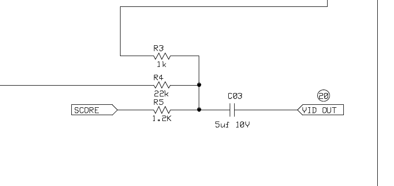
Replacing it fixed the issue.
Board works!
