
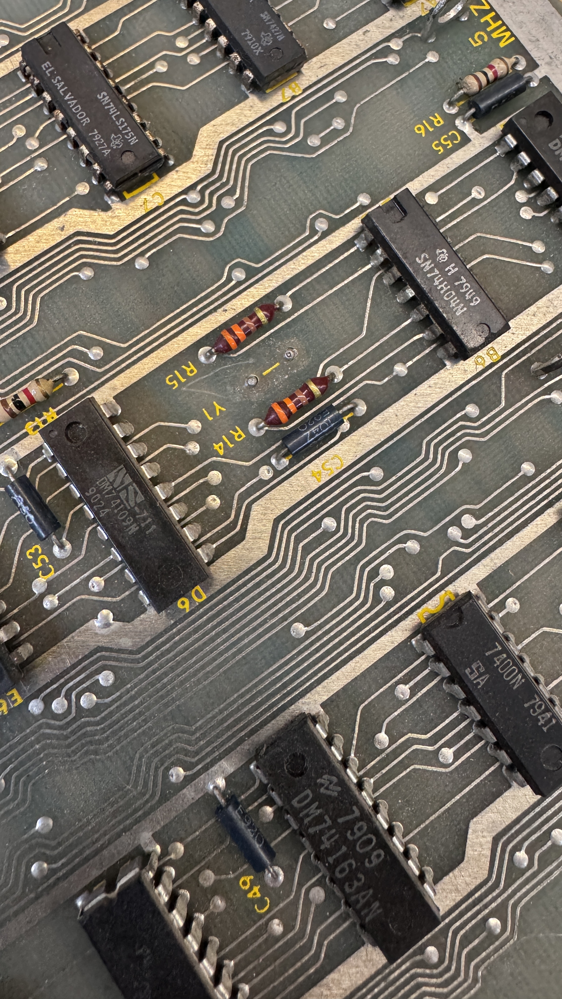
*** Newest Entries always added to the bottom ***
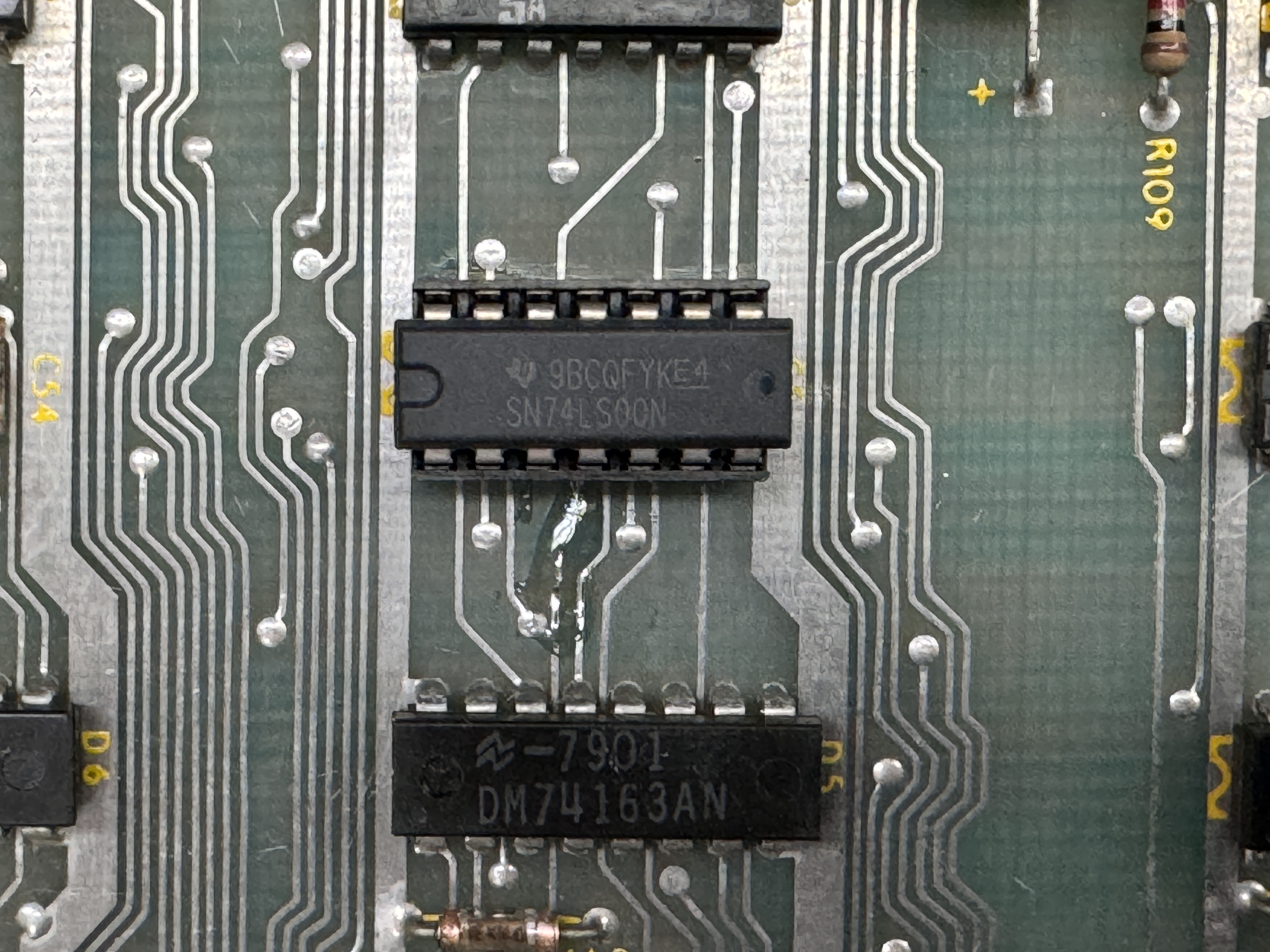
I’d picked up a handful of Missile Command PCB’s a while back to add to my repair list.

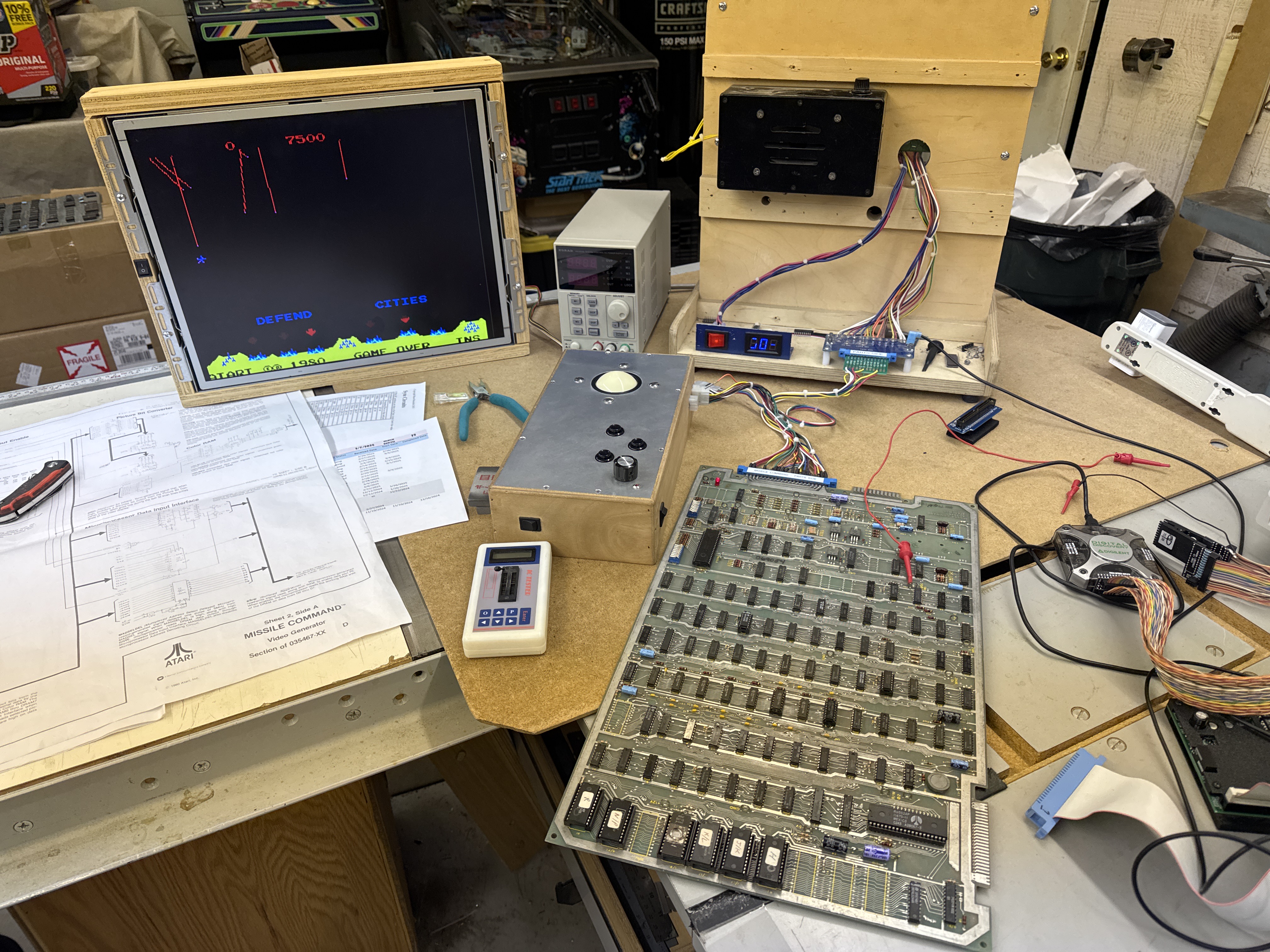
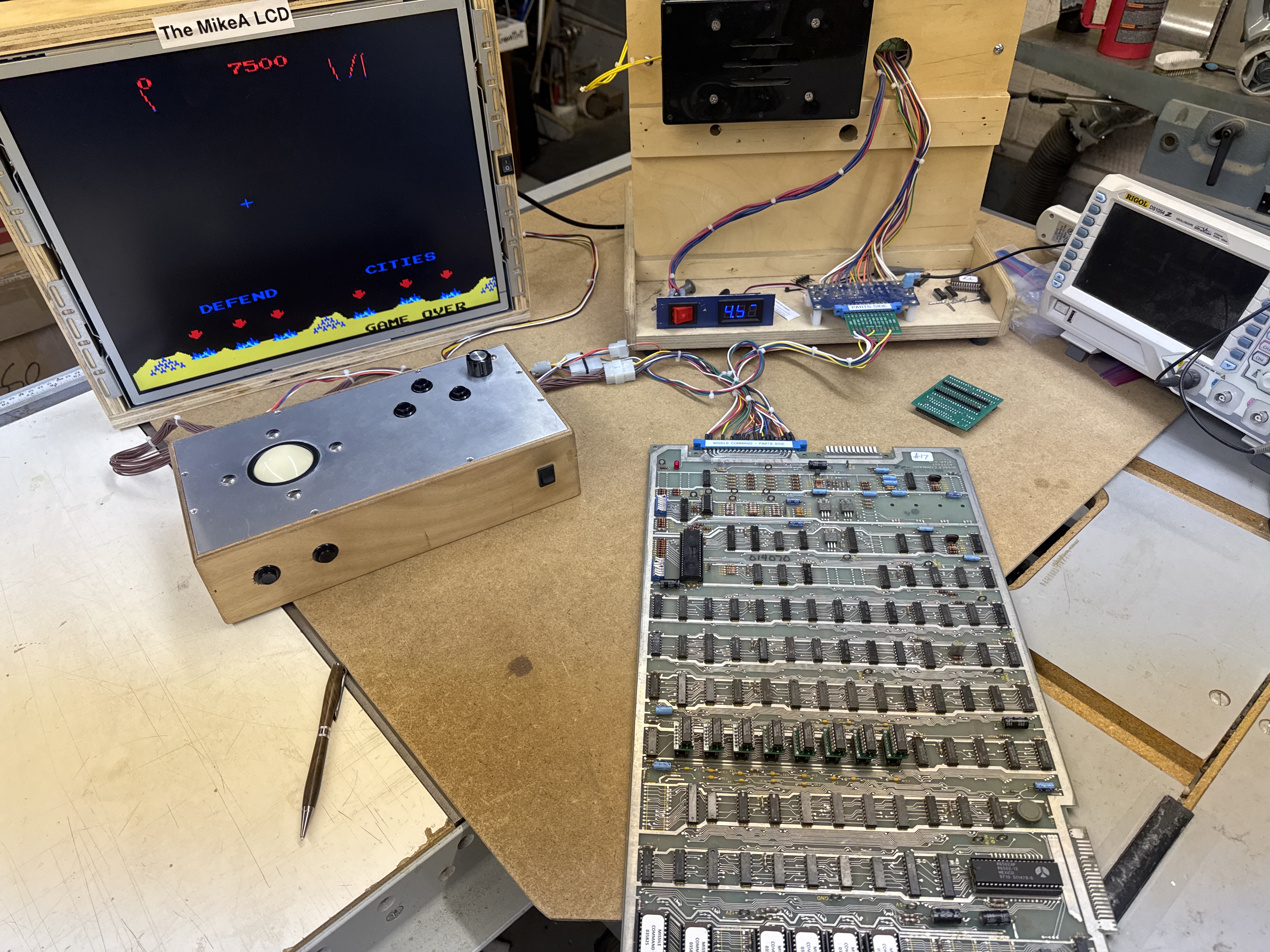
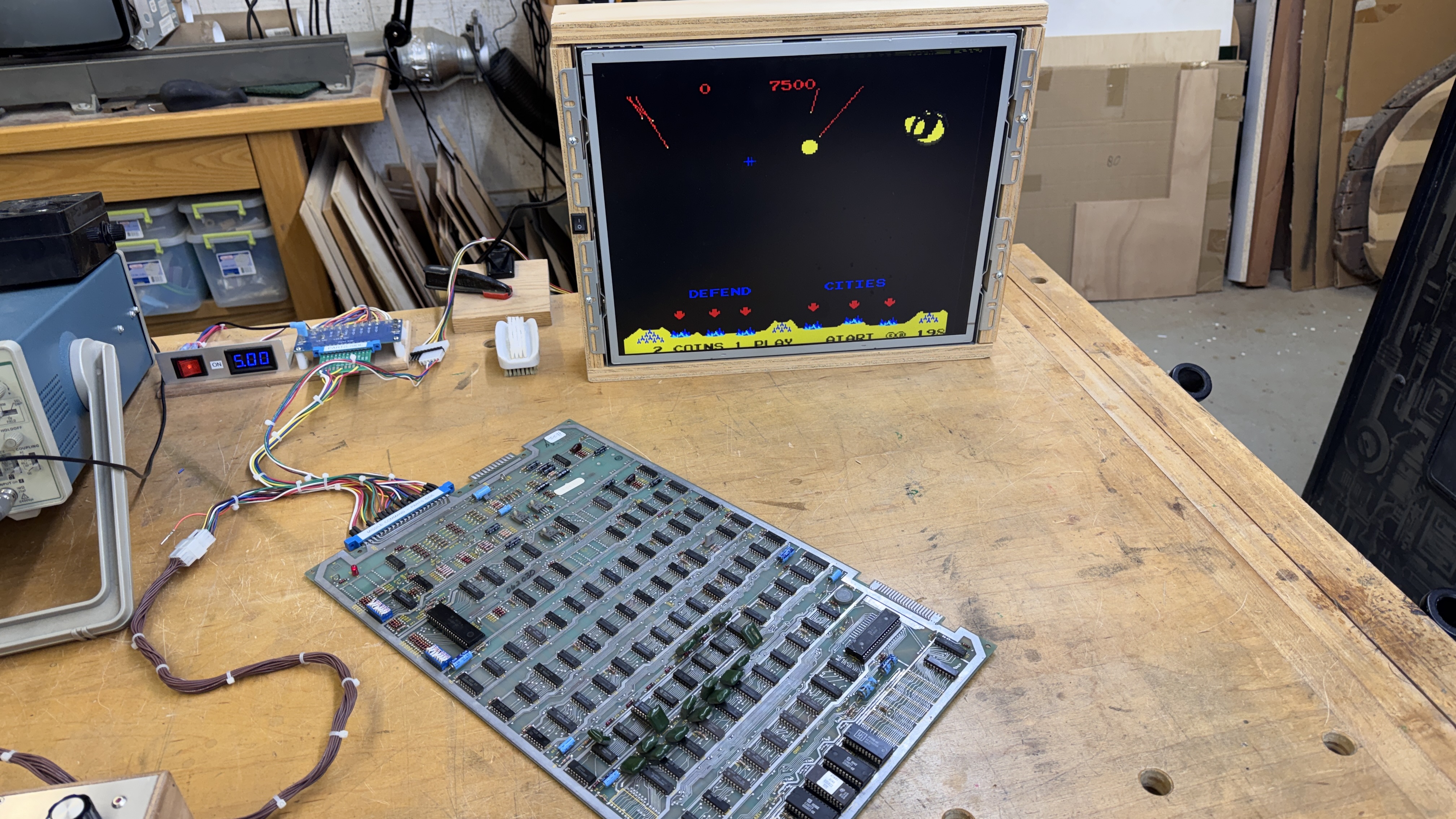
My Atari Bench Power Test Rig has made creating adapters for each board I work on relatively easy. I can typically build one in a couple hours. Swapping between different game boards on the bench now takes all of a few seconds. It’s extremely useful when swapping between two or three of the same board to compare signals when something isn’t quite right.
Changing from Missile Command to Star Wars to Tempest is a quick adapter swap. No need to double check power connections, verify that things aren’t backwards or hold my breath when I power on a board. Between the adapters and the controllers – I’ve saved a lot of time being able to move between boards quickly.
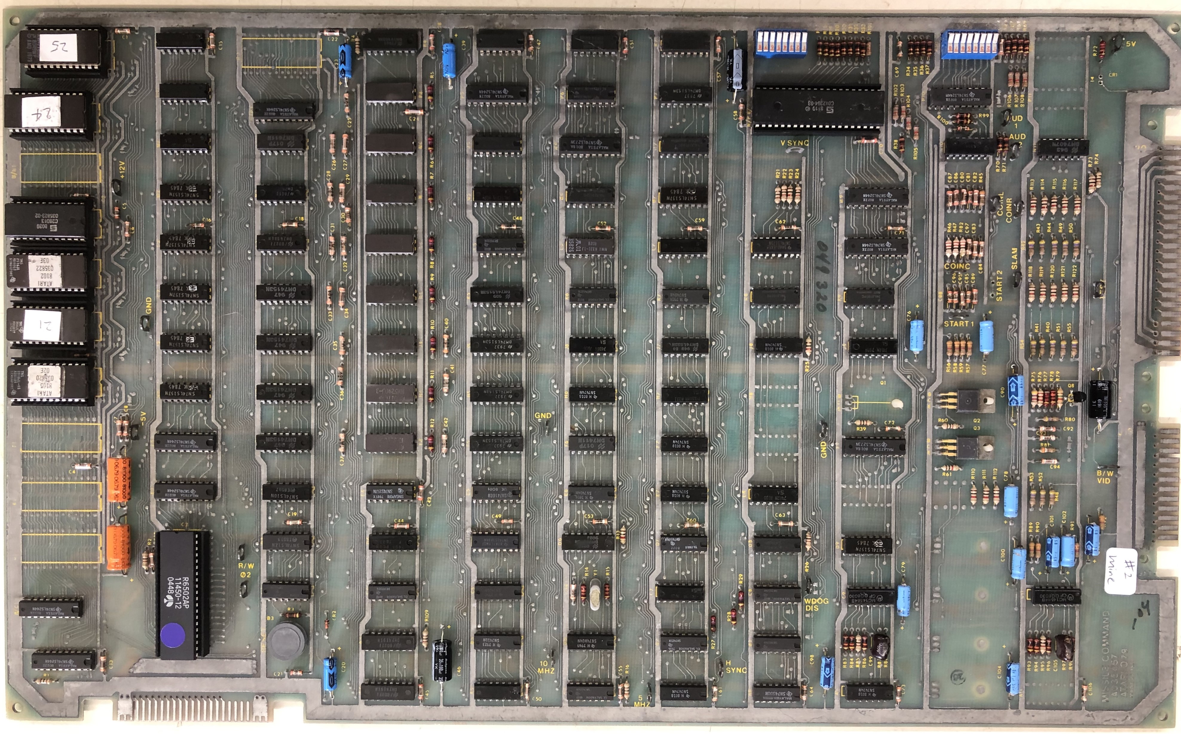
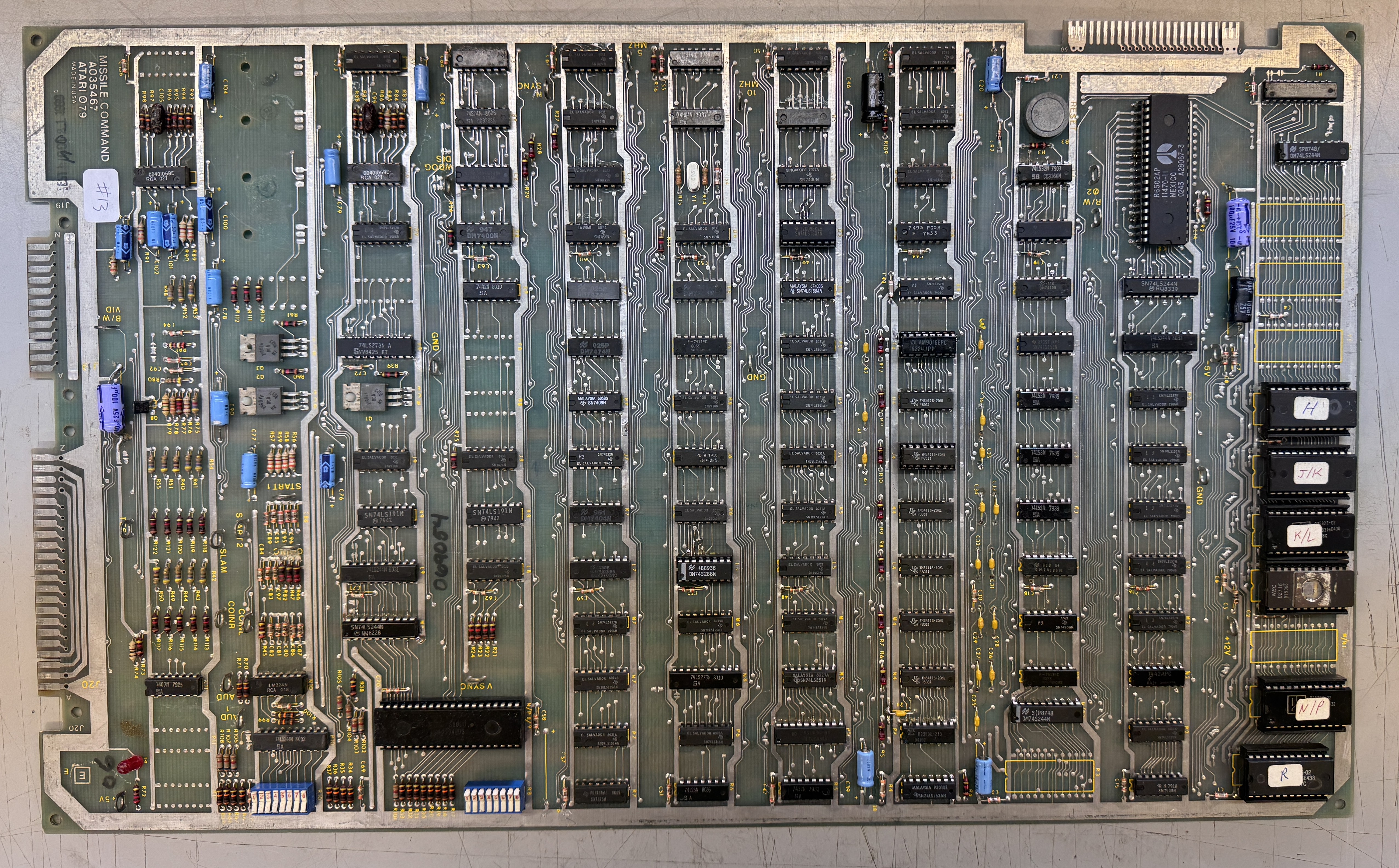
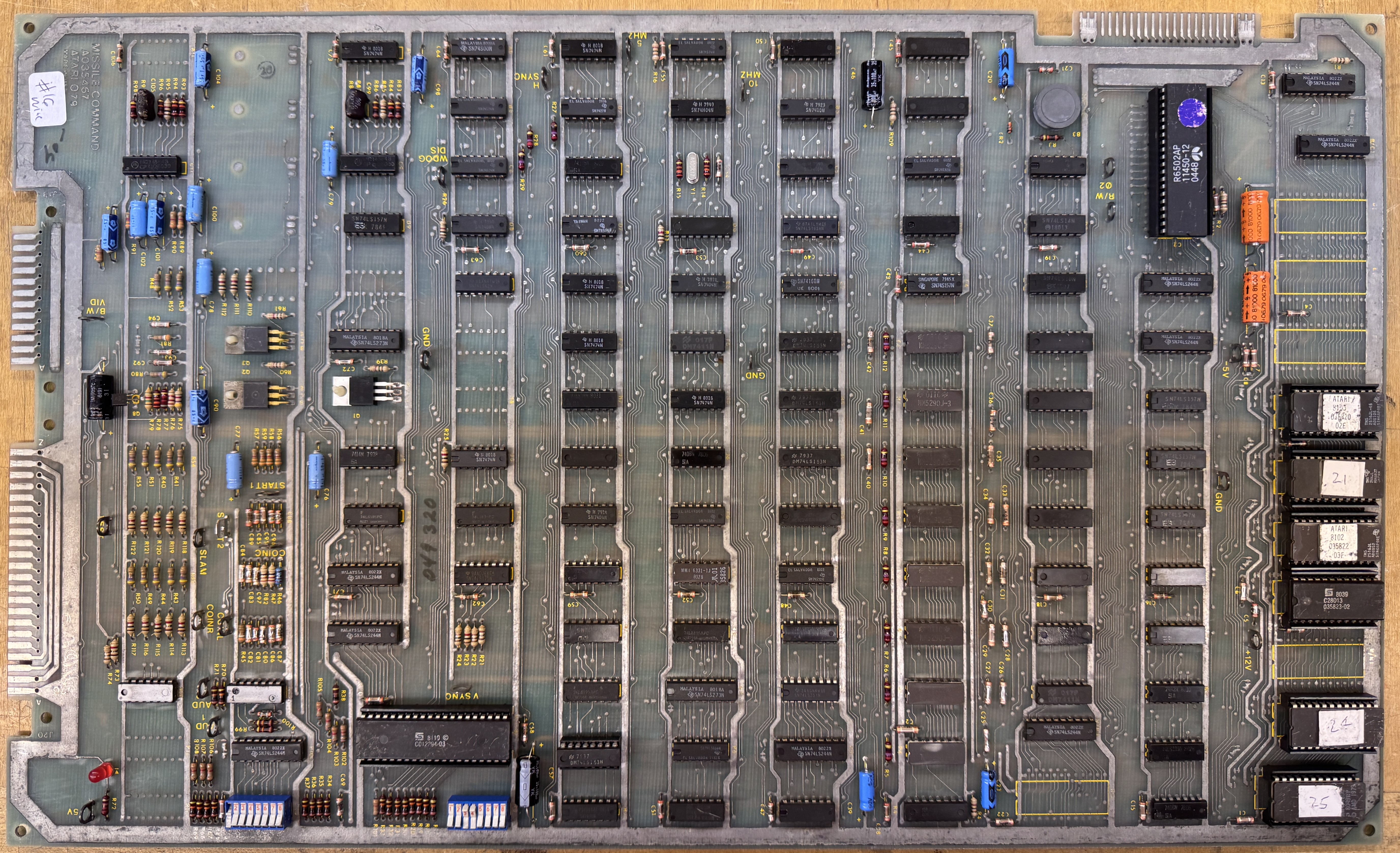
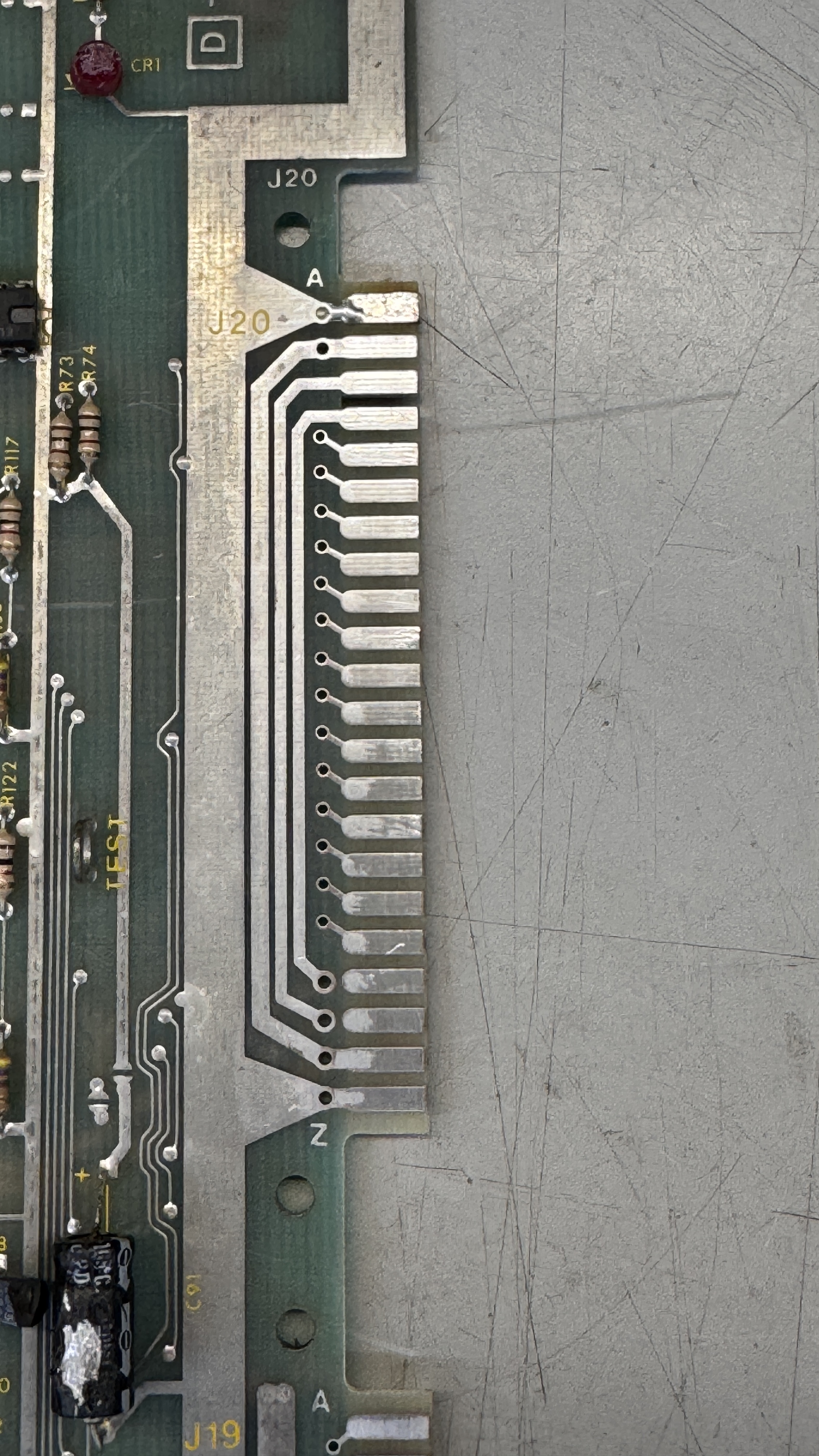
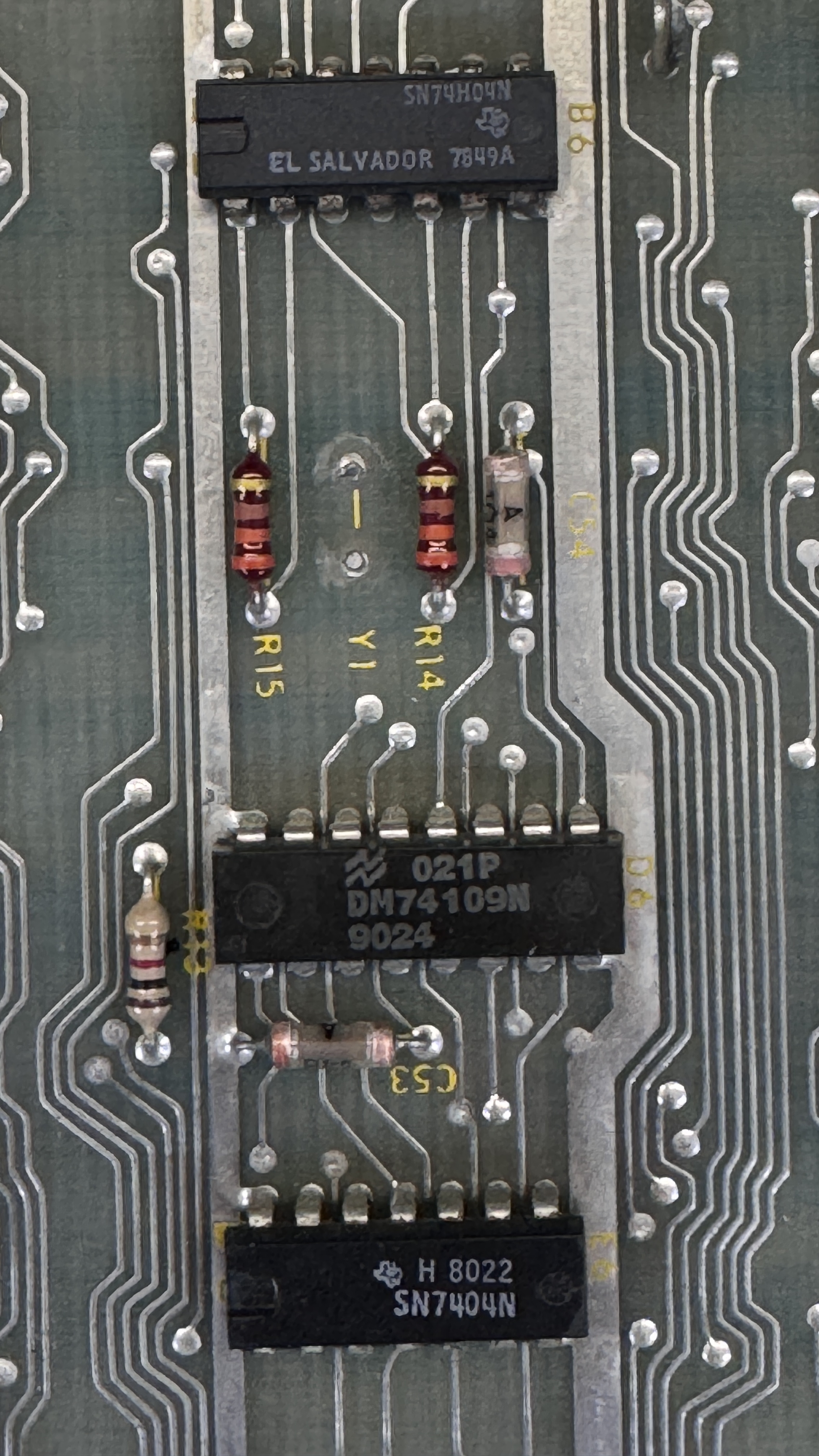
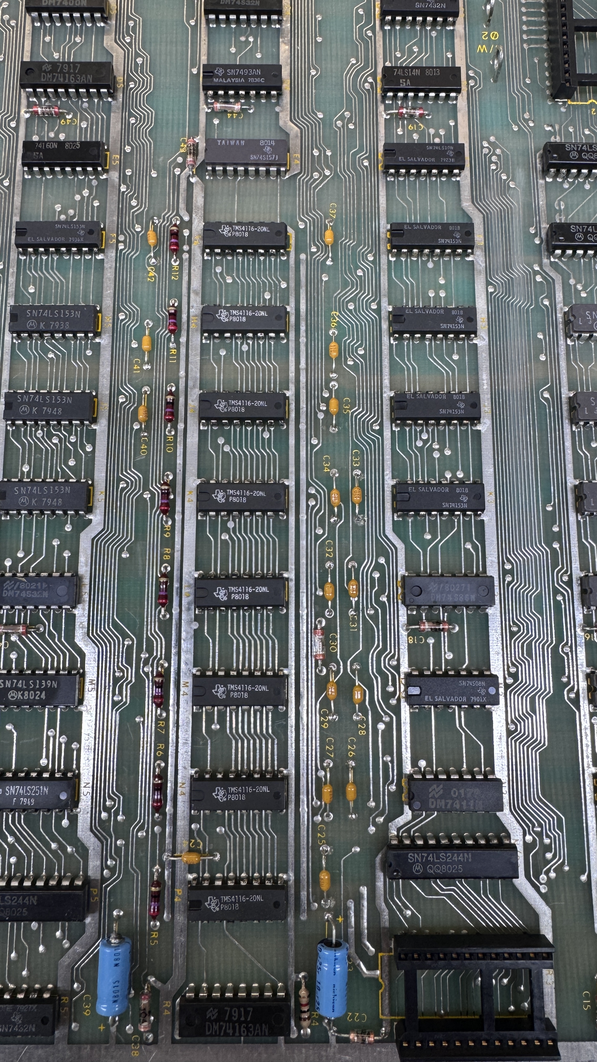
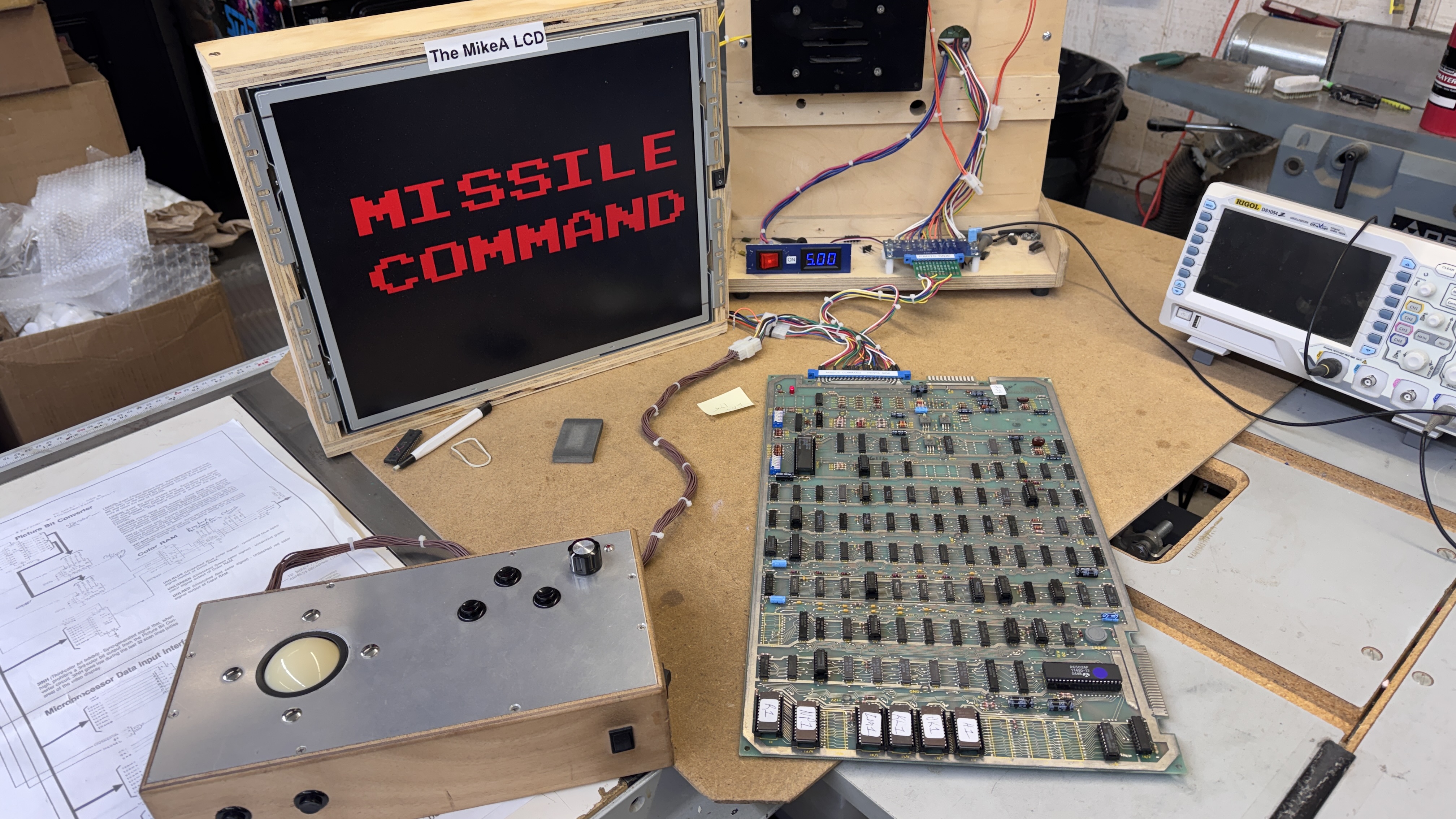
Board #1 – One of my boards
I wanted to test my new adapter after verifying the pinout.

Triage:
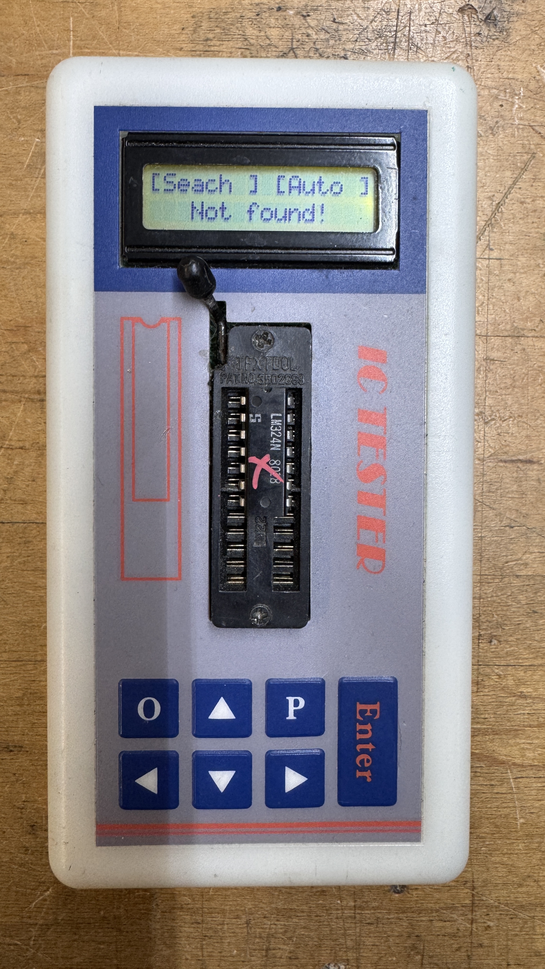
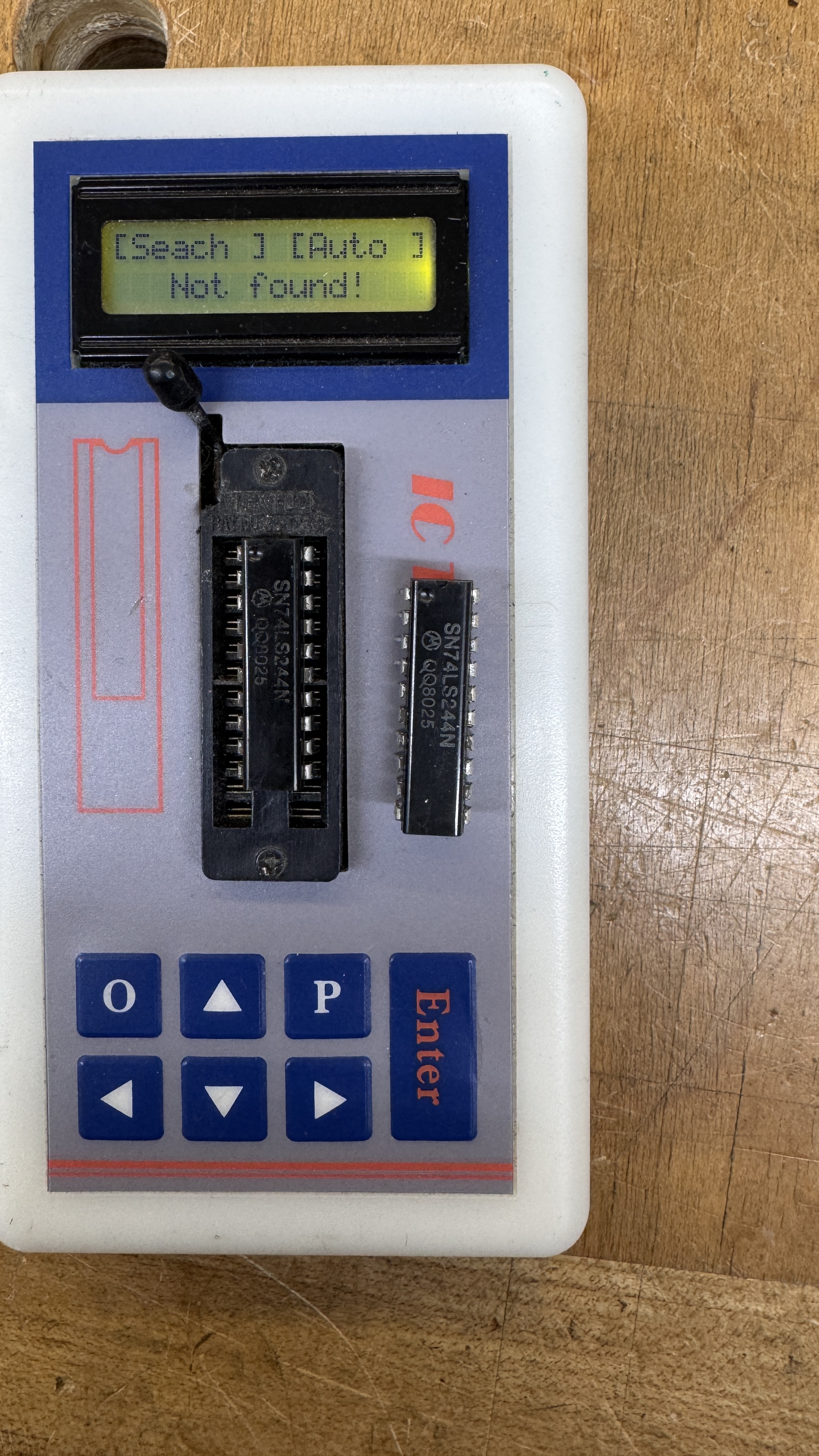
- RAM/ROM check with the FPGA CATBOX – all good
- Crystal had been replaced with one that was almost right.. 10.250 MHz.. I replaced it with the correct one.
- Connected the board and the game runs upside down, backwards and green.

First thing to check was FLIP. Turns out that OUT0 was not active. I followed that back to here:

Here I determined that the LS42@E8 was not getting a BA10 signal. BA10 was working properly everywhere else on the board.

Prior work! Someone had socketed and replaced the LS74@J8 and cut 2 traces. Repairing the traces restored BA10 to E8.

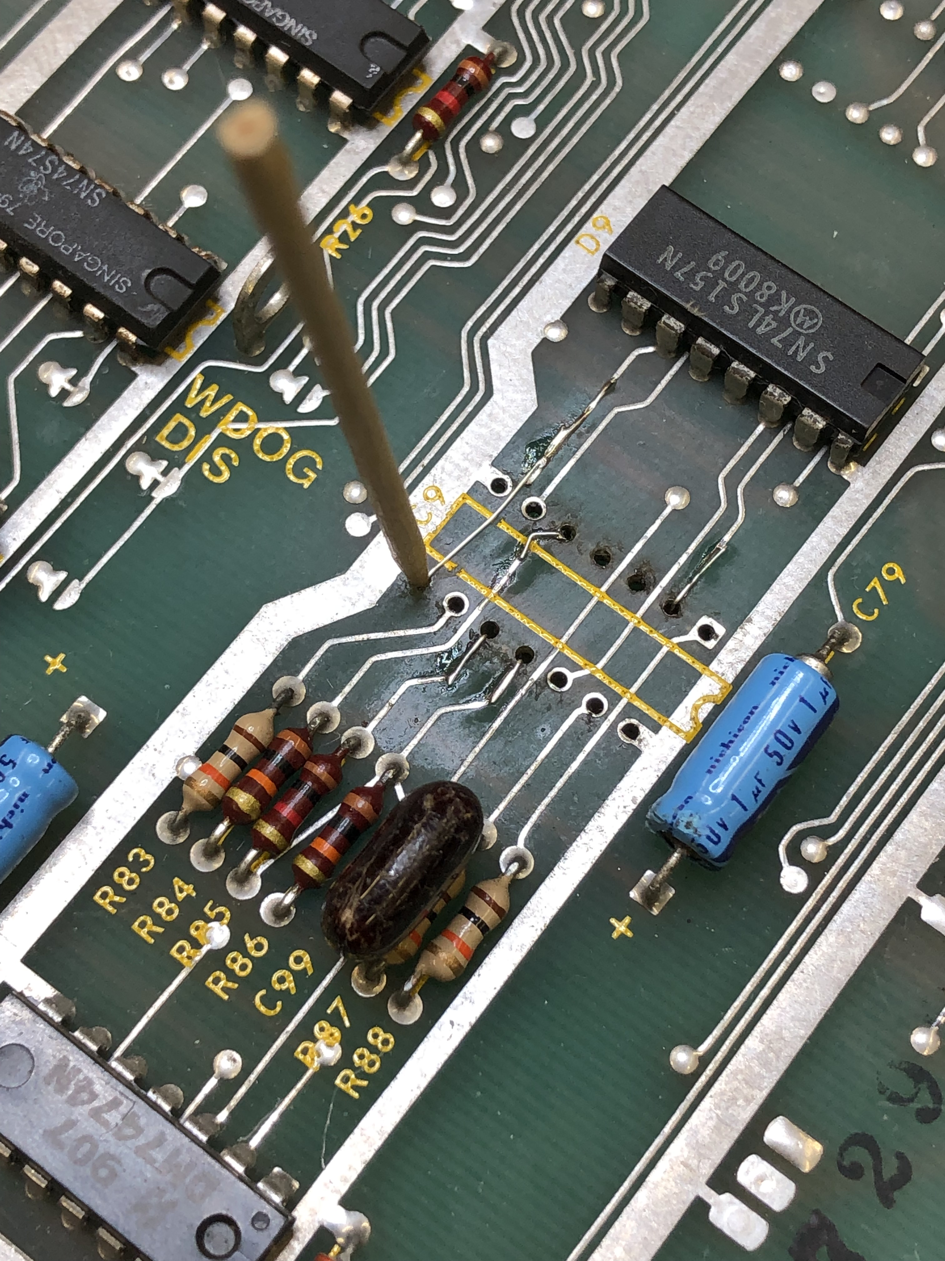
Game works – the trackball was not running well horizontally. I started with the chip @C9. It was socketed and was a 74LS14. The original chip was an MC14584B. The 74LS14 is similar, but not the same. I picked up CD40106BE’s – which are a suitable replacement. But got only a marginal difference. There was a socketed 74LS157@D9. I swapped it and there was no real difference. The socket was a real cheap one. I removed it. After looking at the 74LS74@J8 seemed to be latching funny. Moving right would studder on the scope and it seemed like the trackball was slipping in a couple of ‘lefts’.

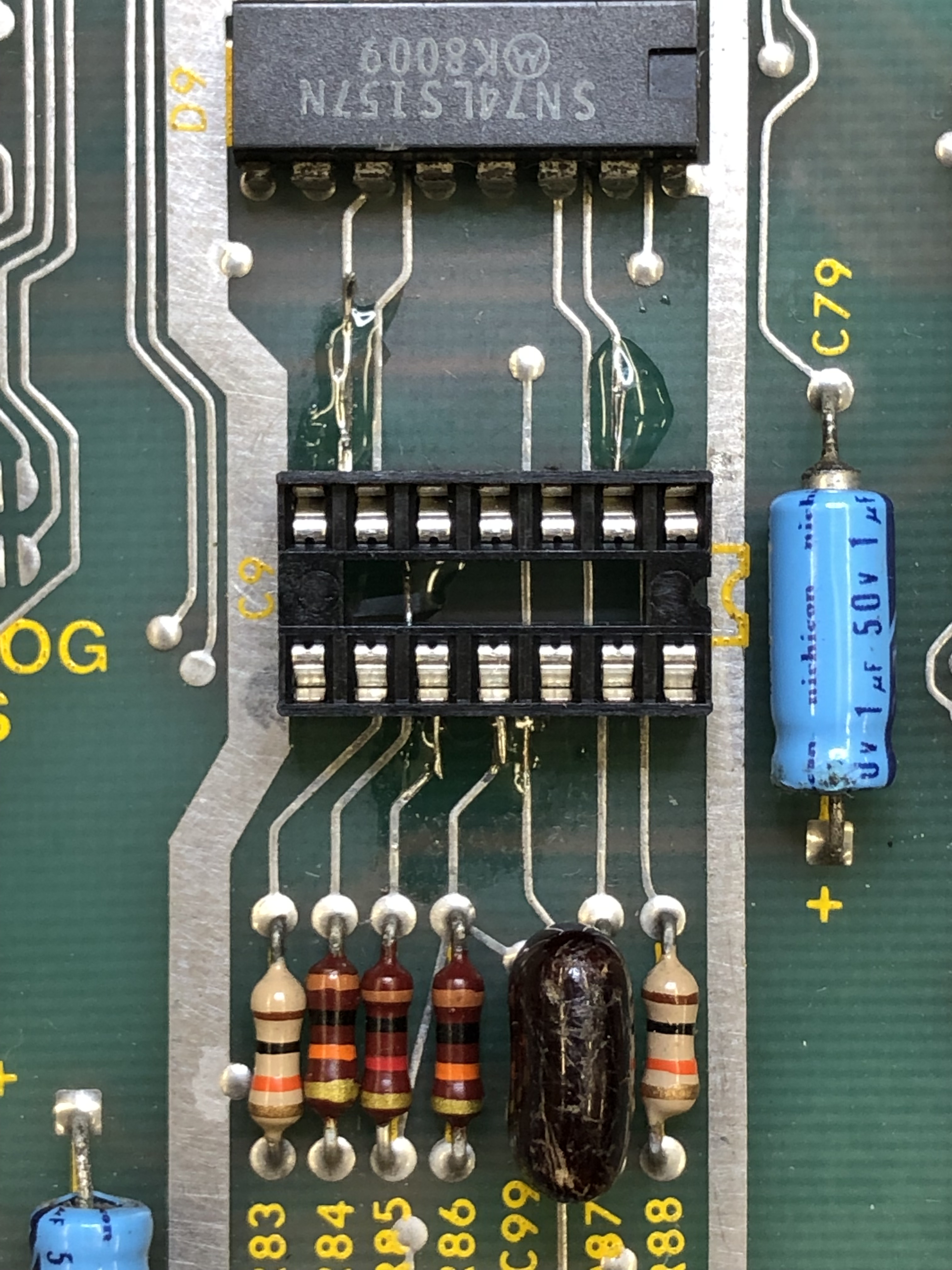
The only thing left were these grey caps, which look like they may have been replaced at some point. I compared the voltages coming from them to another board and they were just a little lower.. possibly right on the border and causing the LS74@J8 flipflop to…. flop now and then? I swapped out the caps @C76,77 which are on the horizontal trackball inputs – problem solved! I recapped the rest of the trackball inputs.
Board works!
Board #2 – One of my boards
Triage:
- RAM/ROM check with the FPGA CATBOX – all good
- Watchdog circuit broken. Needs to be disable for the board to run
- Color Blue missing
- Red, green muted color (it seems)
- Power LED missing
- Missing Q1 – coin counter transistor
This one is a bit older looking – haven’t washed it yet. I wanted to get it going to help diagnose the trackball issue on the last board. After checking RAM/ROM – I checked all of the sync circuit frequencies and the carryover bit on LS163@D5 Pin15 was 2x what it should be.

LS175@L8 had no output on Pin2 – Replaced it and got the blue back. Overall the colors are muted so there is more going on. Connecting to my PVM – the colors get cut off. Replaced Q8, no change. Need to keep poking around.
Still need to look at the watchdog circuit – but I was able to use this board to help investigate the trackball issue on Board#1
Repair still in progress – on the shelf for now..
Board #3 – One of my boards
Triage:
- Missing reset button
- Missing MC14584B@C6 – traces torn up.
- Prior work in many places


I’ve run into a number of boards recently that have had the on-board reset button removed. They are pretty much useless once the game is inside the cabinet – but when under repair on the bench – I use it quite a bit. Found a perfect replacement since the originals are no longer available. Get the Amazon – Atari Replacement Reset Button – When I got them – they were $5 for 100. Can’t ask for better than that – $.05 each!
I have shredded traces to repair @C9
Checking RAM / ROM – RAM checked fine (with an exception).. The ROM was weird – If I inserted the ROM@H1 it checked fine, but J/K1, K/L1 and L/M1 checked bad. If I removed H1 – the other 3 checked good. After checking signals – the select line for H1 was upside down so it was nearly always enabled. Prior work to blame as expected. I went around the back of the board and cleaned up many solder bridges like this one. ROM errors cleared up. One interesting side effect was when H1 was installed – a RAM error on RAM7 would trigger.

I went through the sync circuit checklist, no issues.
(insert my sync list here)
This board also had trackball issues – LS191@K9 was bad. Seems the Missile Command trackball may be tough on the PCBs? A couple of my boards have had a fair amount of work that is trackball related.
Repairing traces with Kynar wire. It’s small work – solder a repair in place with wire bent down through the via. I clean up the flux with alcohol and then use a UV cured resin to lock the wires in place. If you don’t they will release when soldering the socket. Once done – it is barely noticeable and indestructible. No wires on the back of the board!

Board works!
Still need to do a full test cycle and verify – on the shelf for now.
Board #4 – Board in for repair
Triage:
- Small amount of prior work
- Reported all 8 memory chips failed
- Broken cap @C29


I removed all the socketed chips, washed and inspected the board. There were a number of places where the parts side traces were damaged by prior work. I cleaned all of these up as I found them.
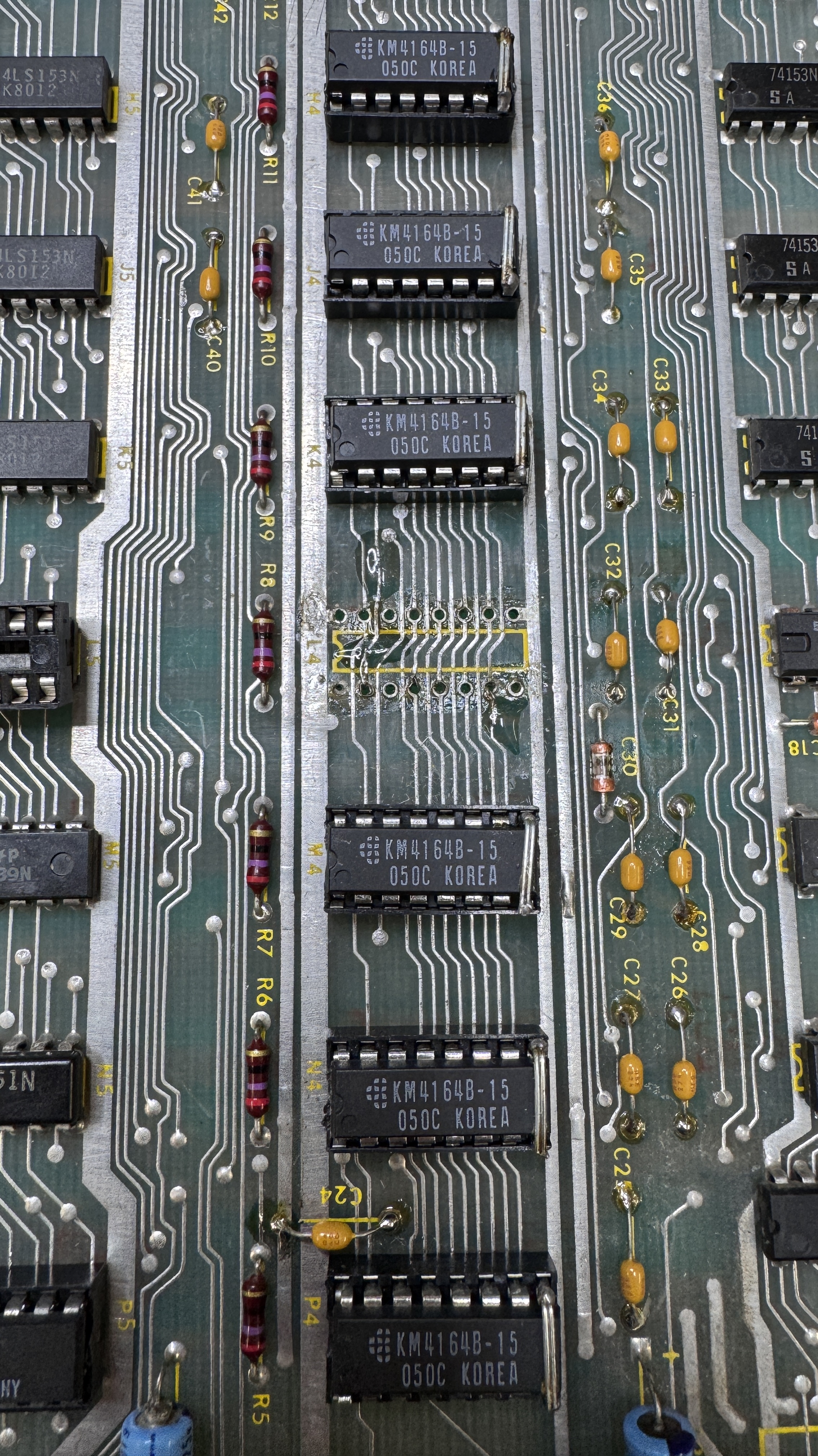
Once powered up – the board beeped out 3 bad memory chips. (@M4, @L4, @H4)
Socketed and replaced.
Board works!
*** Update ***
22 hours into testing, the 5th RAM failed out of the original 8.
Socketed and replaced the remaining 3 RAM.
Burn in testing completed without additional board failures
Board Works!
Board #5 – Repairing a board for a friend
He got a great deal on a full size Missile Command cab that wasn’t working. Sent me the board and the ARII to check out.
ROM@H1 was rotten, during cleaning, two more had legs that broke off.


Once powered on – we got here. The CPU was also bad and unfortunately the Pokeys legs were all rotten. Most were barely holding on.
CATBOX showed some bad RAM@P4, L4 – replaced. At this point I figured I should be hearing beep codes. There were none.. Replaced LM324@N10 – diagnostics running and we have beeps!
It was beeping out RAM H4, J4 – socketed, replaced – no joy..

Replacing the 74153@F3 restored the address lines selecting DRAM0, DRAM1 – RAM test now works.

Board works!
Board #6 – Board in for repair

Board is in nice shape. None of the caps are broken off.. I remove the Braze kit for testing.


A little prior work here – the trace on pin4 of this socket was broken and jumpered on the back with this wire. I generally remove these and repair on the topside. These wires should be fine, but can snag and break loose.
A little Kynar wire and some UV resin to lock it in place and this is much less susceptible to damage. Initial testing showed that the first 4 ROM were not readable. All RAM was good.

LS00@C5 – Pin11 Bad output on the scope. This turned out to be the socketed chip. It was an off-brand chip that was labeled 74LS00, but reads 74HC00 in the tester. These chips sometimes work and sometimes do not work. It depends on the circuit they are in.. Replaced with a Texas Instruments 74LS00.
I ran my full test cycle with no resets or issues. As a final check, I put the off-brand chip into the board with the Braze kit – the board locked up within 10 minutes.
Board works!
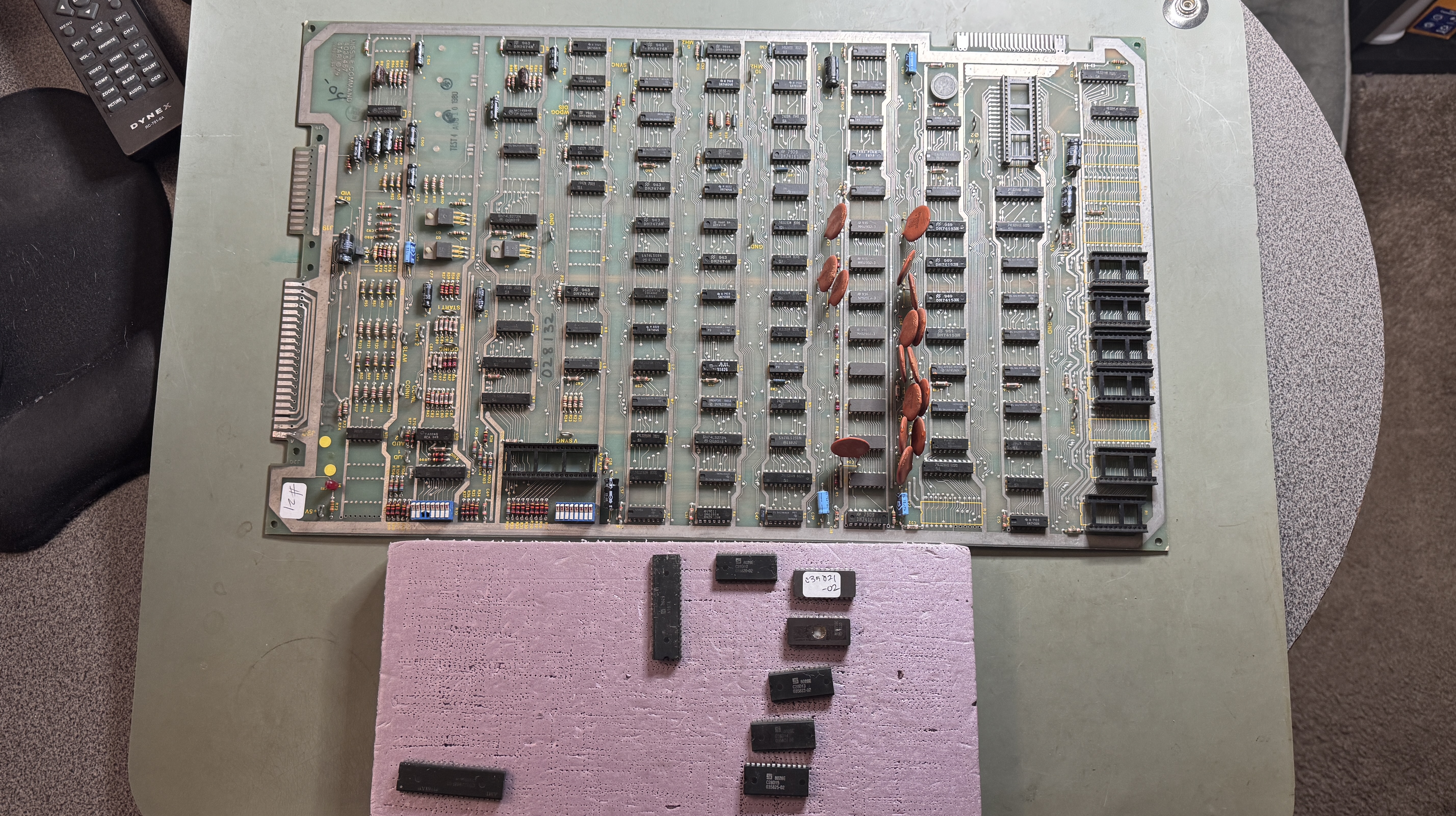
Board #7 – Board in for repair

Board sent in from an arcade. This one is a backup PCB is my understanding. Reliability is the primary concern. Interestingly on this one – it has the full set of 2708 EPROMs. I do not have a reader that can even bench check them – the FPGA tester can do it however.
The 6502 was missing and there was a shorted trace under the socket. C24 is missing and the crystal was broken.
Initial testing showed that none of the ROM or RAM worked – except the single masked ROM reported working.. Weird.. I determined that the EPROMS were not getting their +12V or their -5V. They were getting ~+2V. I first thought it could have been a shorted cap (of which there are many) I had inspected the board looking for shorts in the traces, but none had jumped out. Finally I pulled out the Leakseaker and found it pretty fast..

This is very magnified – I had looked over the board and just missed it.. Snipping these restored the +12V and -5V to all the EPROMS and they all verified! Pretty fortunate IMHO.. As I converted it to 2716’s, I discovered the single mask ROM was a 2716 and was not powered with -5V, 12V. The board had it jumped from the factory as a 2716. Odd.. and explained why it read properly.
Once I got it all checked out…

The boot screen looked normal(ish) but the game screen appeared in Atari 2600 mode.. I probed around the circuit and could trigger different colors, etc. I worked my way backwards and found a PROM..

The PROM@L6 controls the write to the RAM for screen display – all good signals in – all dead out. Replaced PROM@L6.
After communicating with the owner – they want it to be as reliable as possible. I will be removing the 2708’s and rejumping the board for 2716’s and installing new sockets for those 6 chips and a new CPU socket while I was at it..
At this point I started the testing cycle. The game slowly deteriorated from here.. Powered over night and it had rebooted, but was still running.. A chip was dying. I left it powered to see if I could finish it off. Eventually the board would not boot at all. ROM and RAM tests were behaving erratically. Sometimes they worked and other times they didn’t. I’d seem similar behavior in the past, bad address decoding where addresses are being selected randomly or simultaneously, corrupting the busses.
Once I decided it was address decoding, I probed around and piggybacked the LS139@M5 and all of the ROM tests started working immediately. Great! Replaced it (without checking inputs/outputs as I should have).. Same issue.. The one I removed checked good on the tester, piggy backed it on the new chip.. Problem resolved again.. ok .. check the pins..
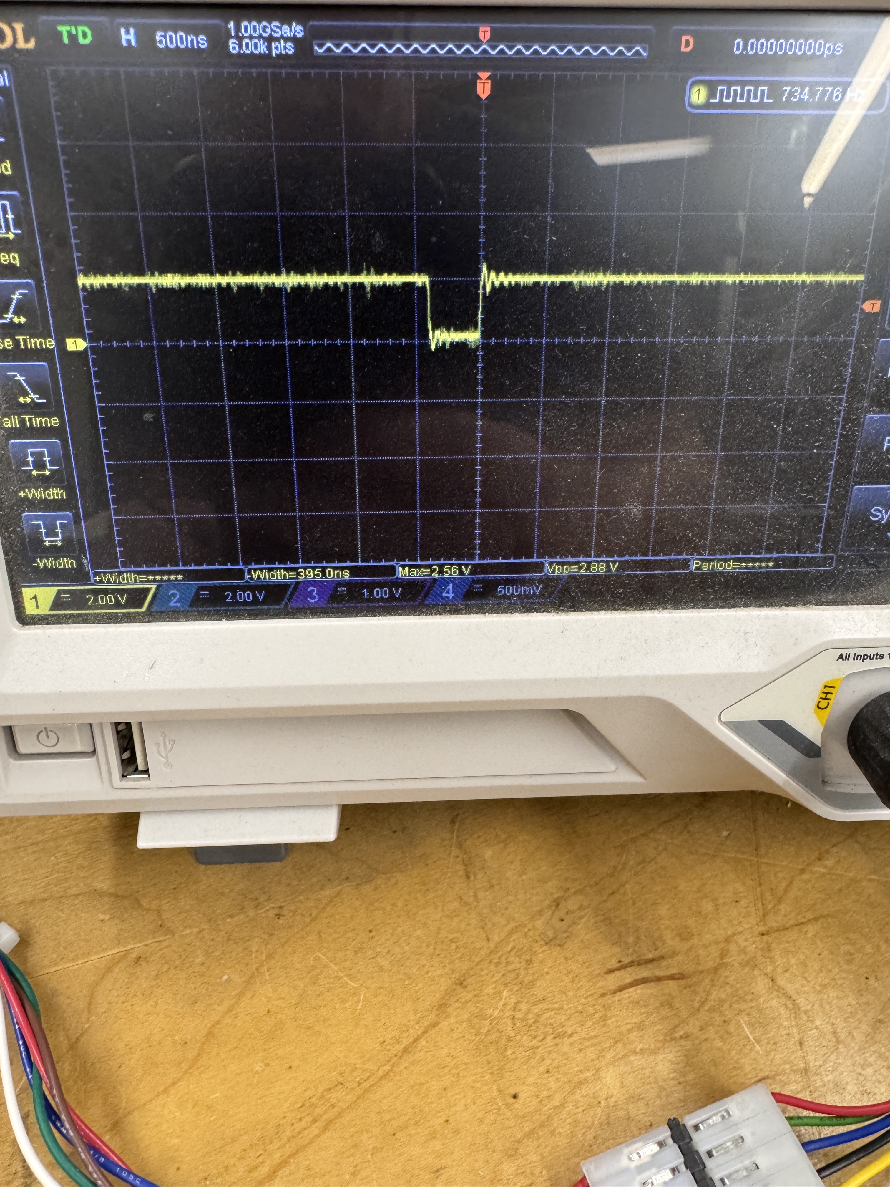
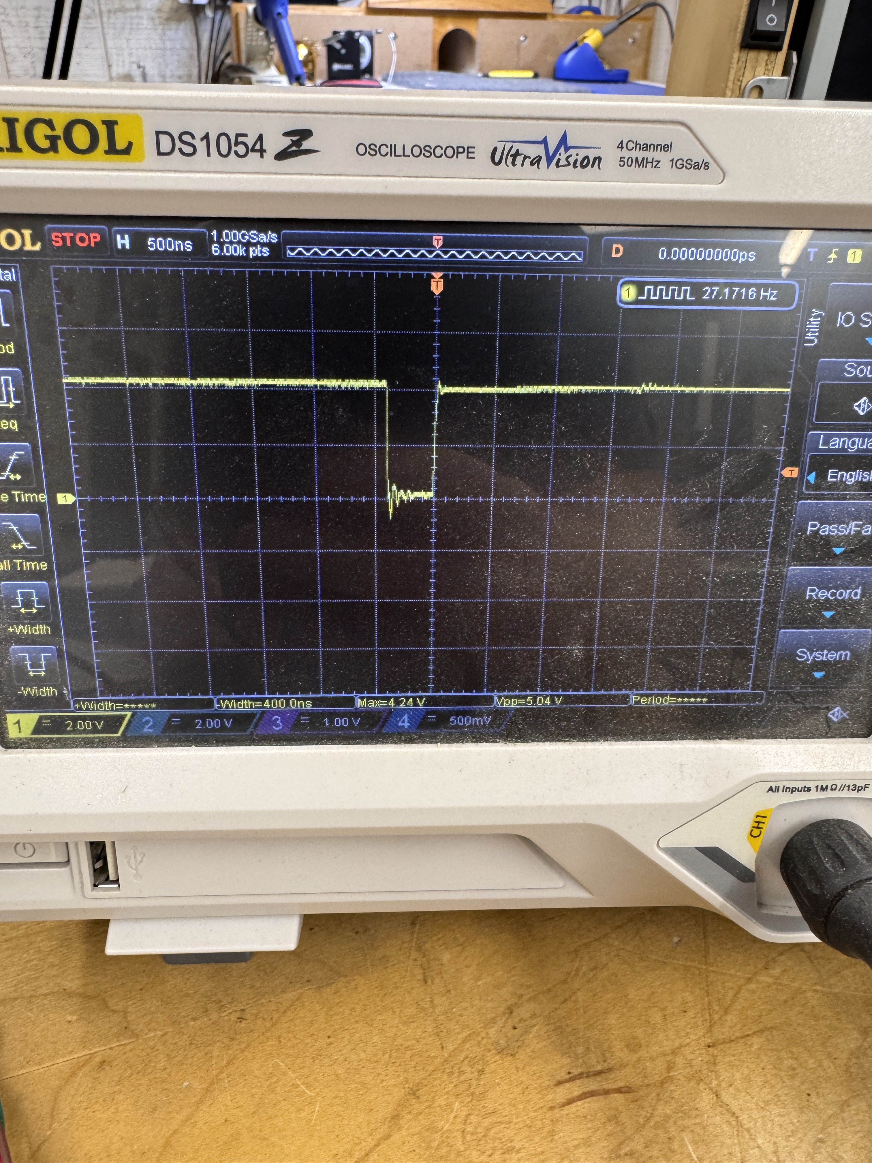
Here is the IN1 signal on the output side of LS139@M5. It is being pulled down by another chip in the circuit. Should look like the signal on the right. Using the meter, this pin was measuring 39 ohms to ground and on a good board it is over 2M.


This LS244@M9 had prior work and is part of the IN1 signal and it appeared it was part of the issue with all of this prior work. I removed and socketed it, but it was not the bad chip dragging down the signal. I cleaned this up as best as it could get..
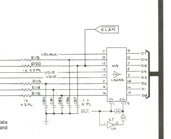
Here is the LS244@M9 that was suspect@Pin 1. After I removed it, the pin1 traces still showed 39 ohms. The only chip left was the 7404@K7 Pin1. The worst part is it isn’t doing anything in this circuit, but it was the offending chip dragging this signal down. Replacing it resolved all the issues.
The reason it effected everything was the LS244 reads the inputs to the SLAM, TEST, and FIRE buttons. Even though they are not being used, the data from them were corrupting the data bus, causing the RAM and ROM failures during test.
Board works!
*** Board came back a few months later. Had a single RAM failure ***
Board #8 – Board in for repair
Owner has started working on the repair and decided to be careful and send it to me. After board maintenance and inspection. I noticed a RAM and been taken out and the second one had one row of legs desoldered. Both are removed here

The RAM@N4 had obviously been pretty hot with the board discoloration. After socketing and replacing. The ROM@H1 was bad. Burned a new one and the board works.
I also replaced the CPU and Pokey socket. They were the original SCANBE sockets, not the best.
**** This one came back with a RAM failure **
Turns out there was more to the story


I’d replaced the RAM@N4 – when it got back to the owner.. He said it was beeping out a bad RAM. I got it back and it worked, then didn’t.. After a little troubleshooting.. pressing on the RAM would get it to work.. I resoldered the socket (made no sense – it was a very clean repair). That did nothing. Found the missing signal going thought R6 or not when pressing the board. A little nudge revealed the hairline crack in the resistor. I’ve had this happen twice in 8 years.. Not an easy to find intermittent issue. These had been worked on prior to me getting the board.
Board works!
Board #9 – Board in for repair
Board reported not working, busted gumdrop caps. Luckily the customer also sent in the ARII.
I decided to connect and test RAM and ROM before doing anything. RAM tested good, ROM was dead across the board. All of the ROMs went in and out of the sockets real hard (so to speak) Chip legs were dirty and the sockets were the Atari gold pincher ones. They work when the board is in pristine shape – but this one was dirty and the chips were not clean.. After pulling the ROMs.

This one had a combination solder splash / smudge taking out the address lines. After cleaning this up, most of the ROMs started to read – but they were flakey at best. Decided to replace all the sockets.

Got all of them off and decided the board needed to be washed. Look close – that is some serious brown.. Cleaning will help with soldering too..

Much better! After installing all new sockets, cleaning all of the chip legs and reassembling the board. Board worked! Until it didn’t. During the first 12 hour burn in – No video output. Game played blind.

7474@A9 is involved with the sync circuit. I’ve had a number of Missile Commands that have chips die very late in the video output section like this. Replaced and the set completed its full test cycle. (almost)
Customer sent his ARII to be checked. It needed a new 2N3055. During all of the testing the sound/volume would be very low or normal.. At first I thought it was the LM324 on the game board – turned out to be the TDA2002 on the ARII was in the process of failing.
During burn in testing (day 3 – It’s been a VERY long time since I had a day 3 failure) a graphics issue developed…
The text scroll across the bottom was sliced up.. I usually think counter when I see this. The missile bases were also off.. I’ve worked on a fair amount of Missile Commands and had not issues on the bottom of the screen. MC treats the last 32 scan lines differently than the upper portion of the screen. All through the schematics there are references to the ‘Cities’ area. Probed a lot of areas around the RAM and the 2H, 3INH signals references and wasn’t finding the trouble maker on this one – Sheet 2 Side A of the schematics is where I had been spending my time…
From experience – I’ve learned not to beat my head against the wall too long when it is not jumping out at me and all the signals seem to be working. The issue had to be on a different sheet…
Looking at Sheet 1 Side B – essentially earlier in the circuit ..
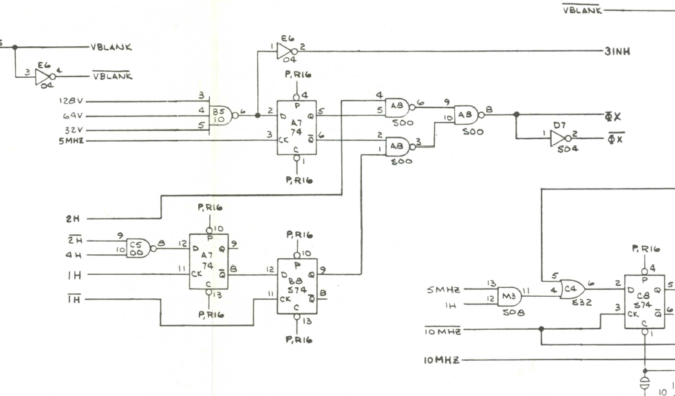
I looked in this area – It had all of the same signals I’d been looking at horizontal counters, 3INH, and the 0X – 0X. Didn’t take long to find 7474@A7 – Pin 8 was dead. Replacing it restored the signals downstream so that the timing would be corrected for the bottom 32 scan lines. Hmmm… 2 x 7474 failures.. I need to check date codes..
*** Decided to do a couple more burn in cycles ***
Good thing I did.. Woke up to the board appearing to be watchdogging.. except it wasn’t. No resets going to the CPU. In test mode it would partially draw the screen showing RAM good, MAP good and ROM good.. then reset before it drew the rest of the screen .. for the most part.
Looking at the schematics – first thing that popped into my head was interrupts..

More 7474’s …….


The 7474@E7 Pin 3 was corrupting the circuit and messing with the interrupts.
One is a failure
Two is a coincidence
Three is a trend…
I replaced all 5 x 7474’s with the matching date codes..
There is a 6th one – different manufacturer..
This particular board was unused for 10-15 years. Many times boards like this have multiple failures after sitting for such a long period.
Board works (again)!
Board #10 – Board in for repair
Forgot the ‘before’ pics. Board was missing the crystal to start – no clock.
Once replaced – checking RAM/ROM – both were showing bad, but reseating and moving them caused different results. Replaced all the ROM sockets, plus CPU and Pokey sockets. Cleaned all the chip legs and did full testing cycle. Board solid ever since.
Board works!
Board #11 – Board in for repair
This one had some other issues. Initially showed a couple of bad RAM. @M4 bit 5 and @K4 bit 3. After socketing @M4, problem remained.. traced it back to a cut trace under the CPU.

Someone used a screwdriver to remove the CPU at some point. Repaired and replaced the CPU socket. The RAM@K4 was interesting – normally when they die – there is no output. This one was working – just outputting bad data. Replacing it cleared the memory issues. After that I replaced all of the ROM sockets (It had SCANBE sockets – had not seen these on MC before, but they are terrible sockets in general).. The Pokey socket was working, but had some damage. Atari gold pincher type – replaced it too.. after that ..
Board works!
Board #12 – Board in for repair

Board 12 and 13 came in together. This one has 54 socketed chips – I expected to be chasing prior work issues on it, but everything seemed to be ok. Connecting to my tester showed a single bit memory error in certain cases. The RAM was good – I could swap it around since it was socketed.

In this case, it was the 74LS153@K3. It creates one of the address lines into the RAM. Pin7 – DEAD6. Replaced it.
Board works!
Board #13 – In with the prior board
This board had a lot fewer sockets, but the prior work was more of an issue and more visible.

The front looked pretty good – but there was evidence of torn up traces and wire repairs in multiple locations of the solder side. First item I chased was one of the traces to the CPU edge connector was broken. I connect my tester to that edge.. Fixed a broken trace on that address line.
Once connected I was able to verify ROM, but the RAM was really messed up.. It would blink on and off on the tester. Verifying the SYNC circuit ..

74LS163@D5 – bad output from Pin15. Replaced it to get E5 running correctly. From here I spent considerable time probing looking for the root cause of the memory circuit getting corrupted. It could have been addressing or data corruption.

The PROM@L6 had been pulled and socketed prior – but something didn’t go as planned. Pins 10,11 were floating.

Removing the socket revealed that nearly all of the vias got pulled out of the PCB. The socket was put in, but the legs were not actually soldered to anything. I repaired the pulled trace and added Kynar wire to the holes with the pulled vias and got the PROM working again. But I still had the issues of the RAM getting corrupted. It showed on the monitor as noise / snow for lack of a better description (forgot to take a pic)
The breakthrough was in this area.

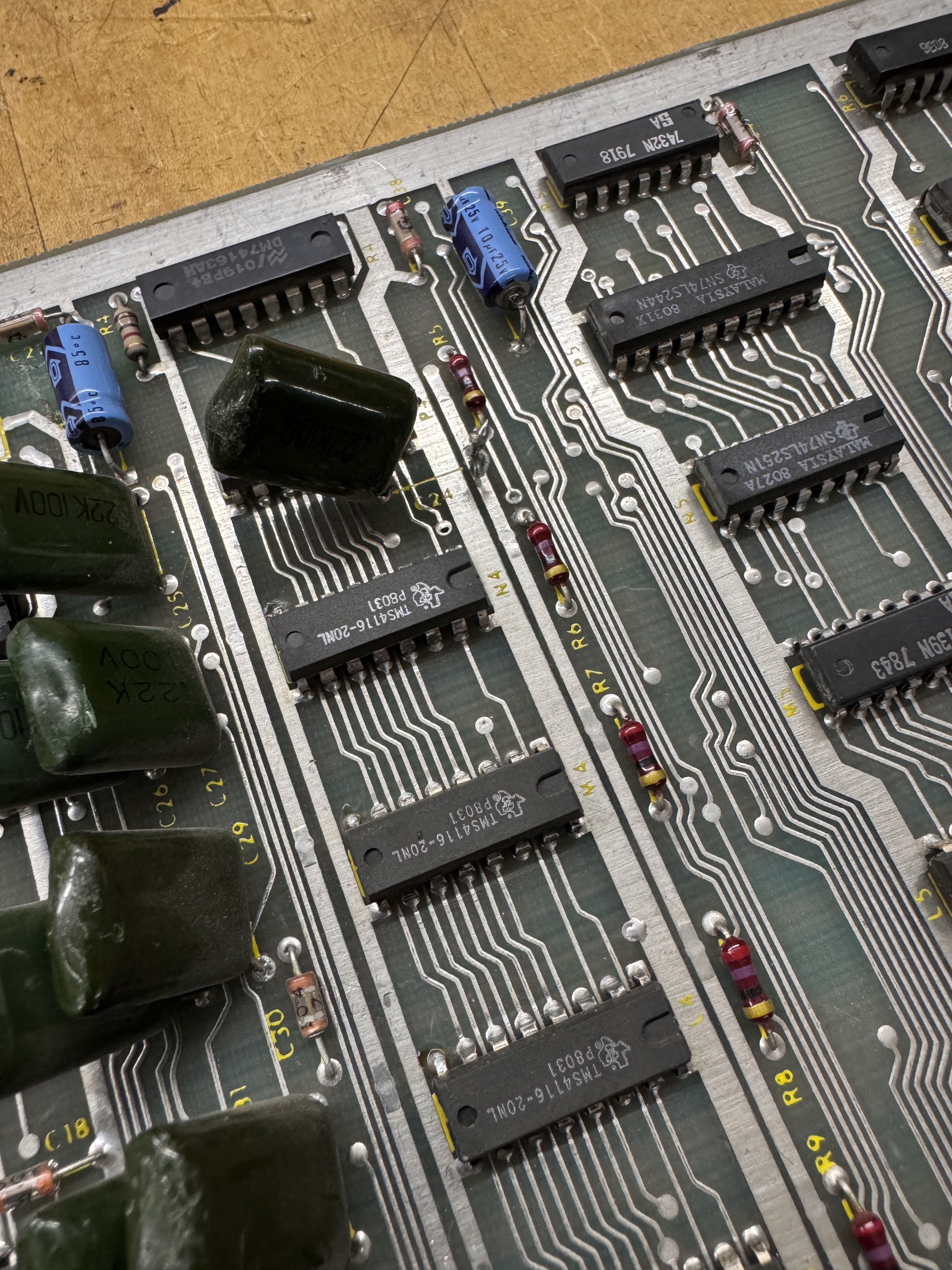
/RAS and /CAS are strobes to the 4116 RAM. That RAM is accessed differently than others.. I tested the frequency of /RAS and it was jumping around at 3.3Mhz or so, the clue was it was jumpy.. It seemed like it should have been very steady just based in the schematic.. Tested a good board and it was a solid 2.5Mhz. 74S74@C8 – pin 5 was putting out a bad signal. Replaced it and the memory corruption was fixed. No more noise. Now I was just missing 1 memory bit.
74LS153@J3 was bad – replaced it.
Board works!
Board #14 – Sent in for repair

Pretty standard looking Missile Command. It has been worked on a few times over the years. Reported issue was no up and down controller motion. But there was a lot going on…


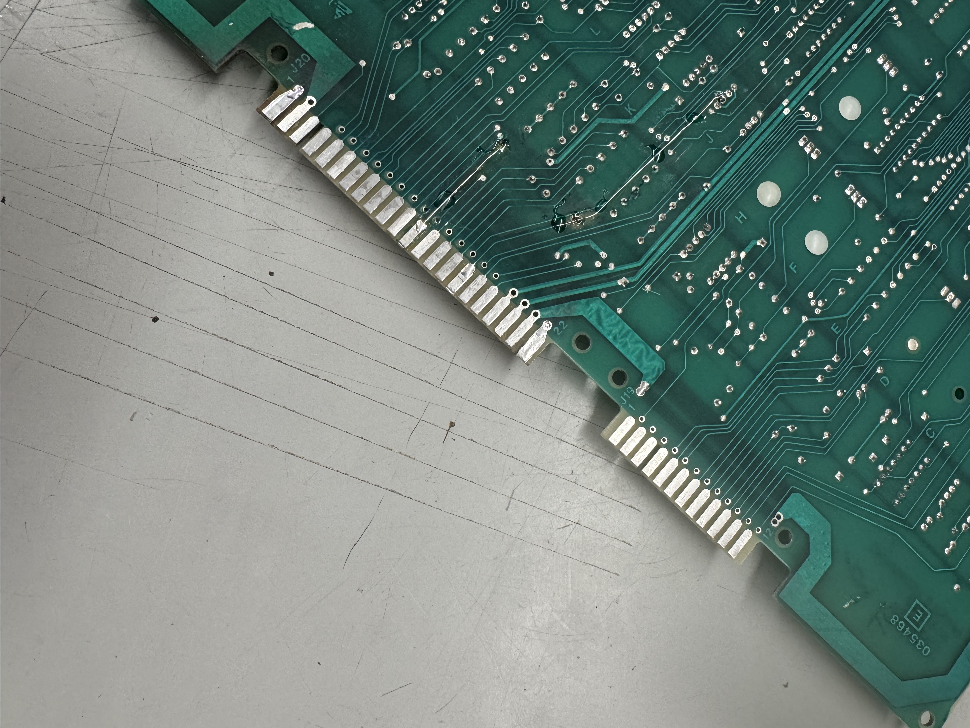
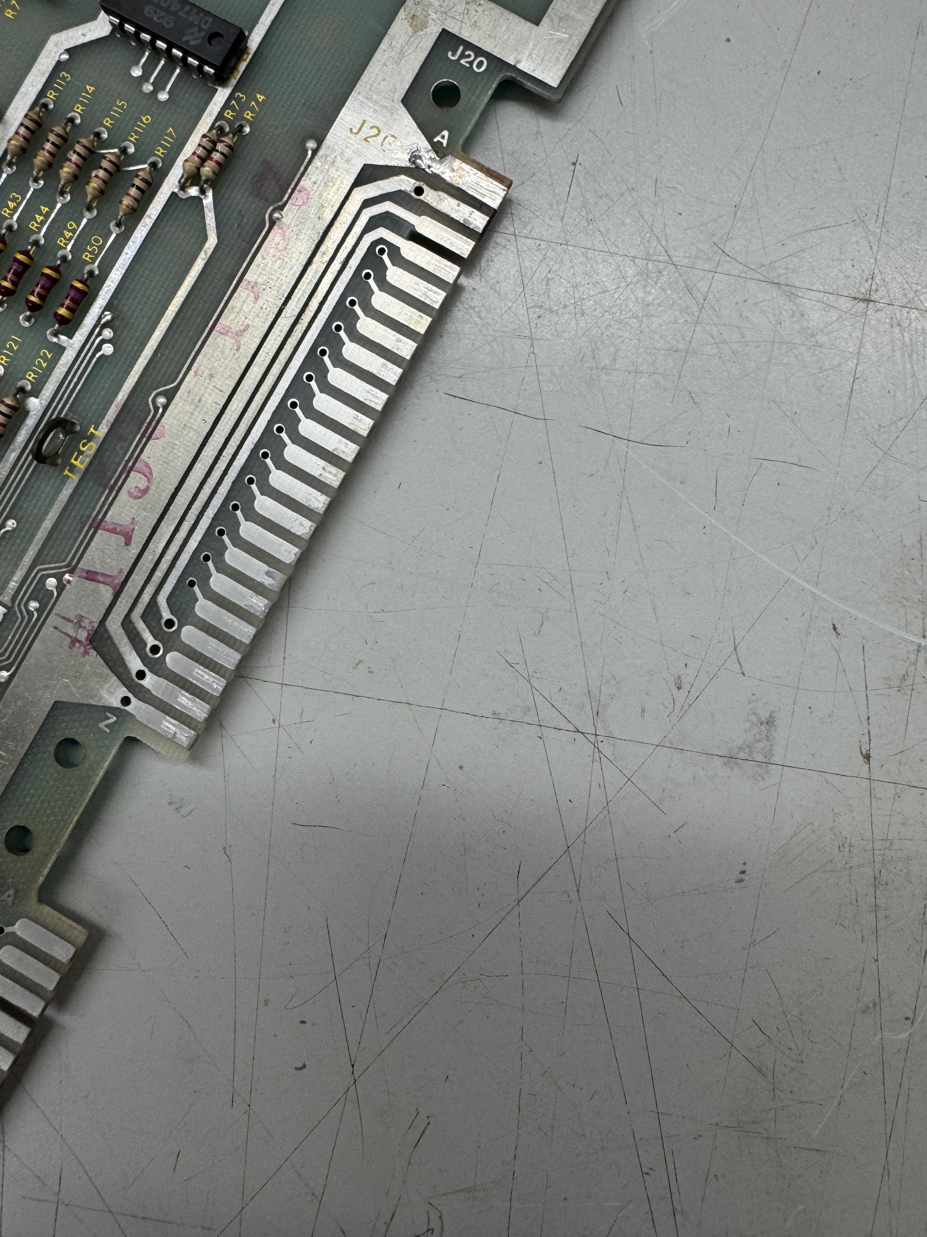
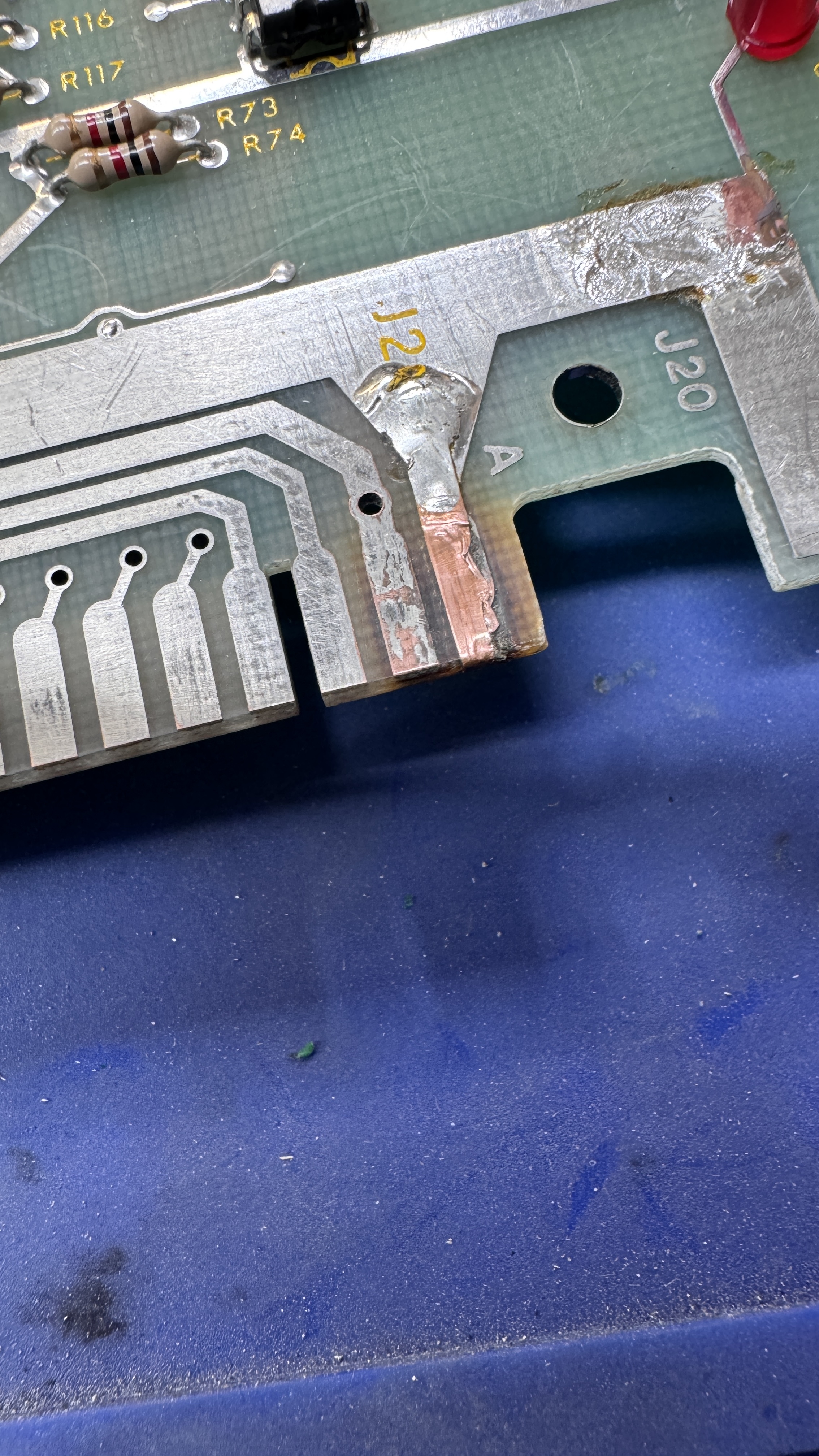
The edge connector was quite torn up at some point.. Thick solder blobs on ground and 5v. Thin strands of wire were used and then green solder mask(?) was used.. but it was uncured.. it came off in sticky globs.. Many of the edge fingers were peeled back and damaged.
Before I could test the board – all of this had to be repaired. There was other prior work..


A small wire jumper (I repaired the trace) and a bunch of sockets were replaced. Lots of flux left behind.. I cleaned all of the green goop off the board, removed all of the stranded wire from below it. Using alcohol and lacquer thinner – spent some time getting the solder side cleaned up. Even then I ended up washing the board to get all of the remaining dirt and flux off.


Here is the edge after cleaning up all of the excessive solder, polishing up the fingers and starting the process of repairing them. The divots get filled with UV resin and copper tape is used to replace the missing fingers. Once they are in place I used Kynar wire to replace the torn up traces.

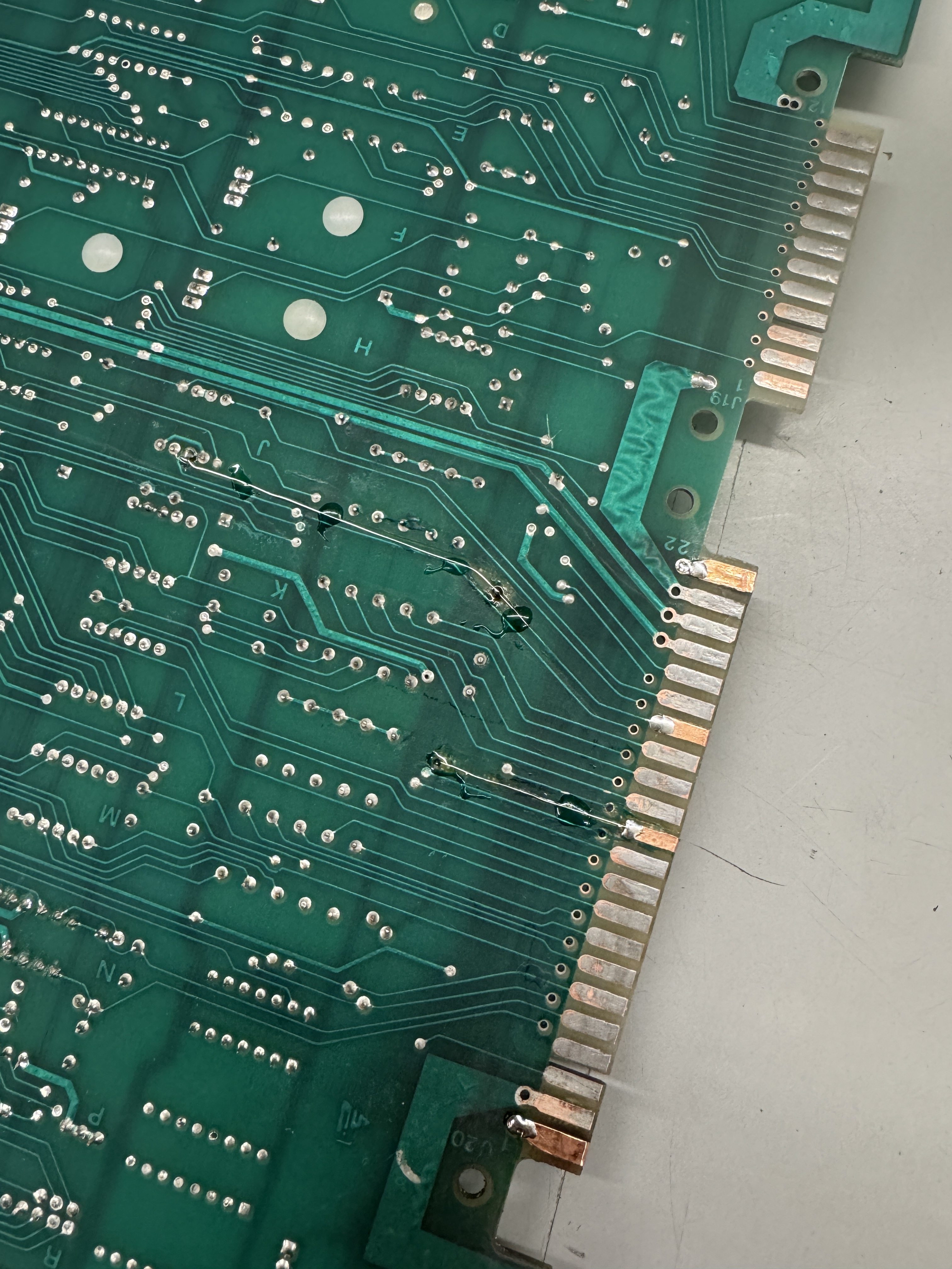
All the copper has been replaced. If you look close you can see the Kynar wire trace repair. It is held firmly in place with UV cured resin and all of the fingers are now of the proper thickness.

Last step – clean one more time and then coat with Liquid Tin. The edge is in perfect condition and repaired cleanly..

Completed remaining board maintenance and replaced a broken cap.
Board works!
Board #15 – Sent in for repair
Board was sent in not working. Did board maintenance first this time.
ROM @J/K1 was bad – burned a replacement and did full maintenance test cycles.
Board works!
Board #16 – One of mine
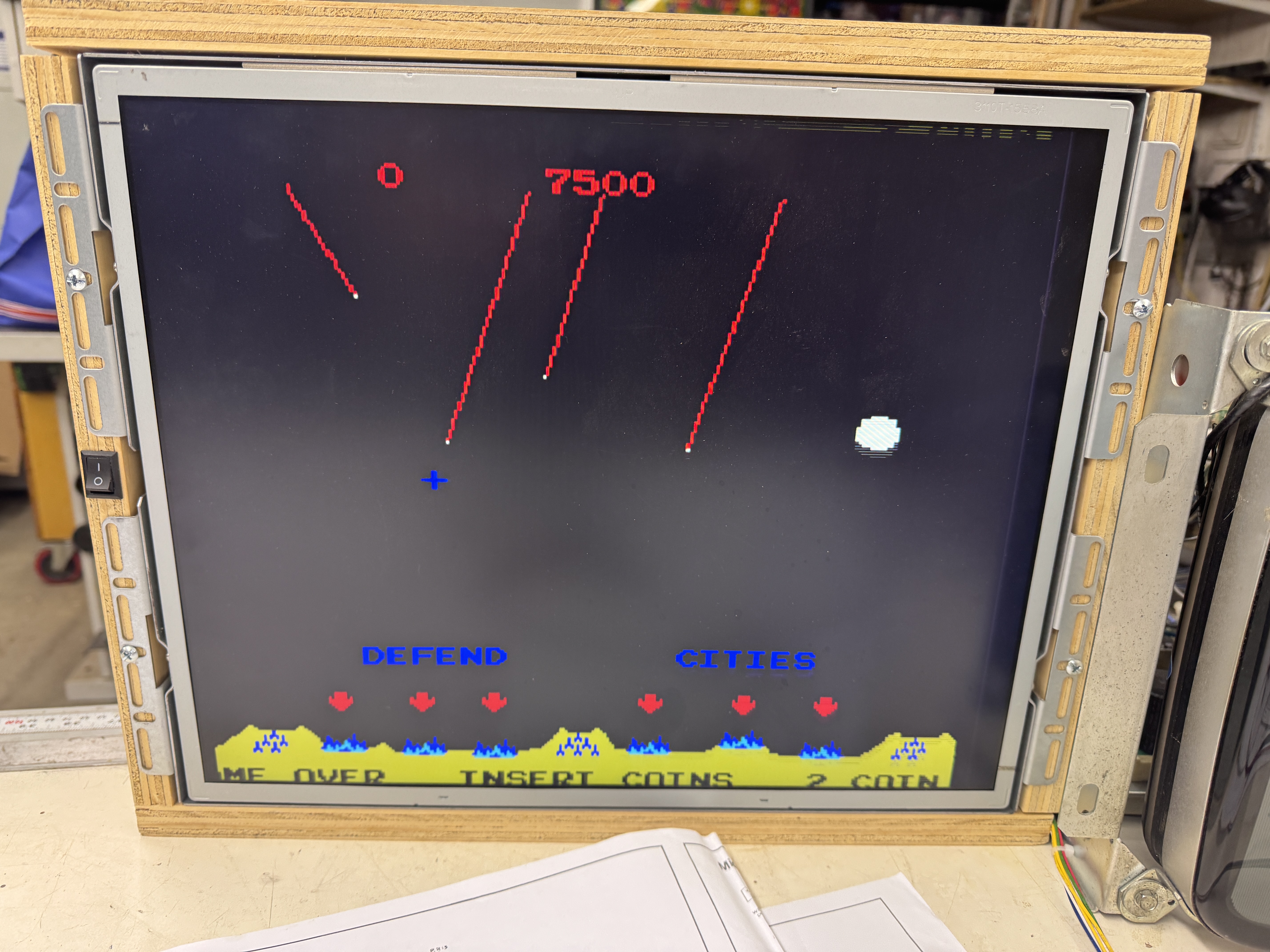
This is the ‘after’ shot. Arcade customer sent in a MC board for repair, Board #17, but wanted a spare since Missile Command is now down at the arcade. I had one that I’d picked up a while back and got it running while #17 is in transit. This particular board had a lot of little things wrong with it.. One thing I do like is the RAM are all ceramic packages. It had no RAM or ROM errors. It’s not the brightest and shiniest board I’ve ever seen. I did wash it.
Items of note:
- Missing Power LED – replaced
- Missing Q1 (coin counter transistor) – replaced
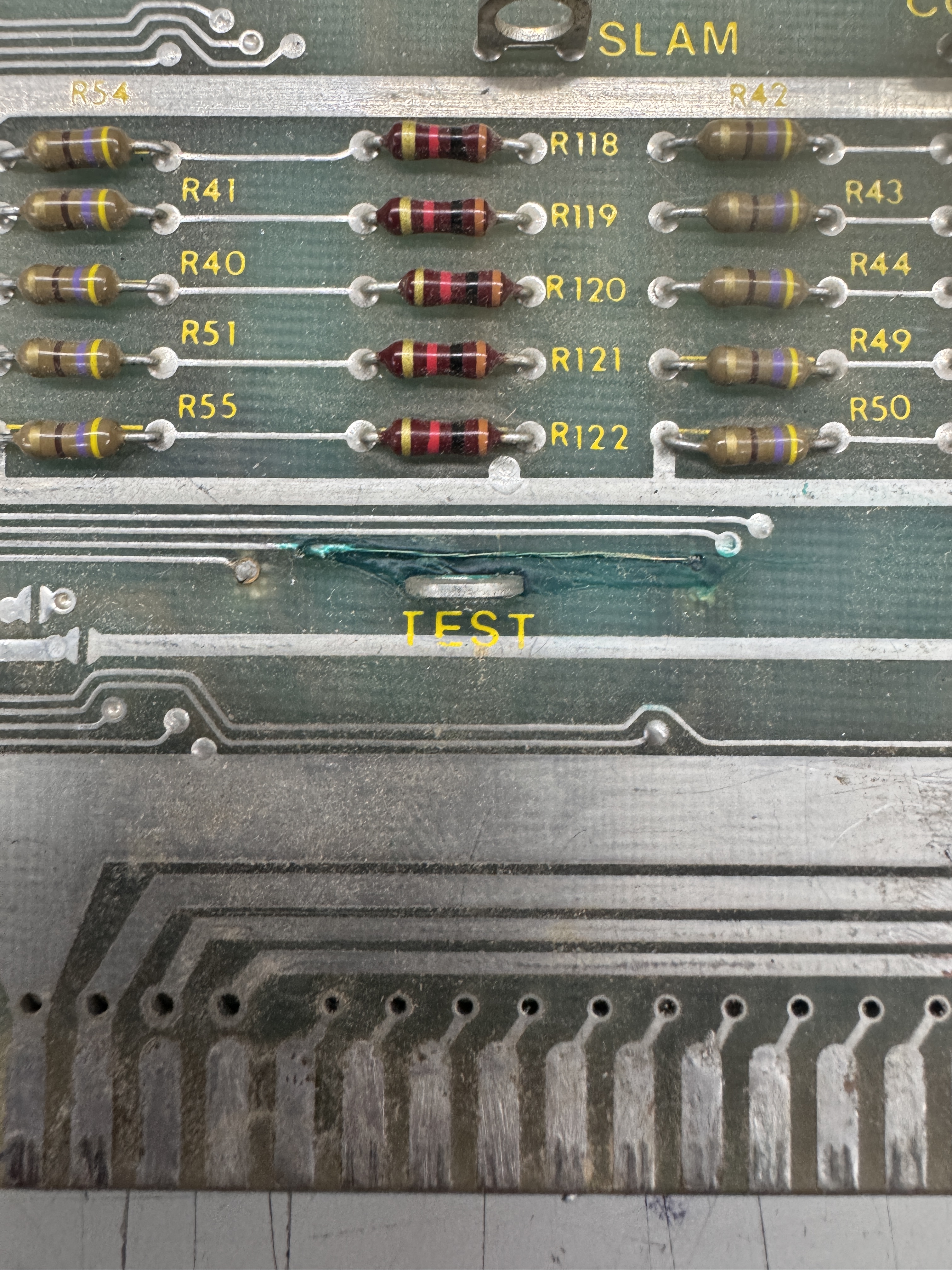
- Start 2 test point was missing – added it because I have them
- Colors were off
- Board was watchdogging
- Cross hairs were leaving trails
- Crystal was fine, the can was rattling – replaced it
- Edge connector got cleaned up and liquid tinned. Copper was a little exposed
On first power up – board was watchdogging. Connected it to the CATBOX and ROM and RAM read good. Disconnected all of that and powered up again – still watchdogging. So I disabled the Watchdog.. board booted. Watchdog needed to be fixed.
Probing the watchdog circuit – the watchdog was not being cleared.. Working backwards..


/WDOG was stuck high going into LS00@D8. It is generated by 7442@E8 Pin5. Replacing it fixed the watchdog circuit.
The colors were off. I determined that it was the BLUE and tested the R/G/B outputs at the video connector with the scope. Working backwards I found the following:

Something that is pretty rare (at least for me).. R46 had drifted WAY out of spec. I could see good ‘BLUE’ signal going in and really bad signal coming out as compared to RED and GREEN resistors. Testing the resistor, it read 2.8K ohms.. not 22 ohms. It was the original – maybe a monitor issue zapped it? Replaced it and colors restored!
The last item was color trails being left by the crosshairs…
This one I did a quick search and found a repair log Game board #16 and it looked nearly identical. One thing about this is it only started after the board warmed a couple of minutes – thermal failure. I sprayed it and some of the other chips in this area with Freeze Spray but the issue didn’t clear.

Repair log said replace the LS153@P7. Before that I did clip onto the chip with a tester and it seemed to effect it. Replacing the LS153 did nothing.. Below that is the LS251@N5. Probing that showed bad outputs on Pin5. I hit this chip with Freeze Spray (a little better than the first pass earlier) and the issue cleared. Replaced it and the color trails were fixed.
Board works!
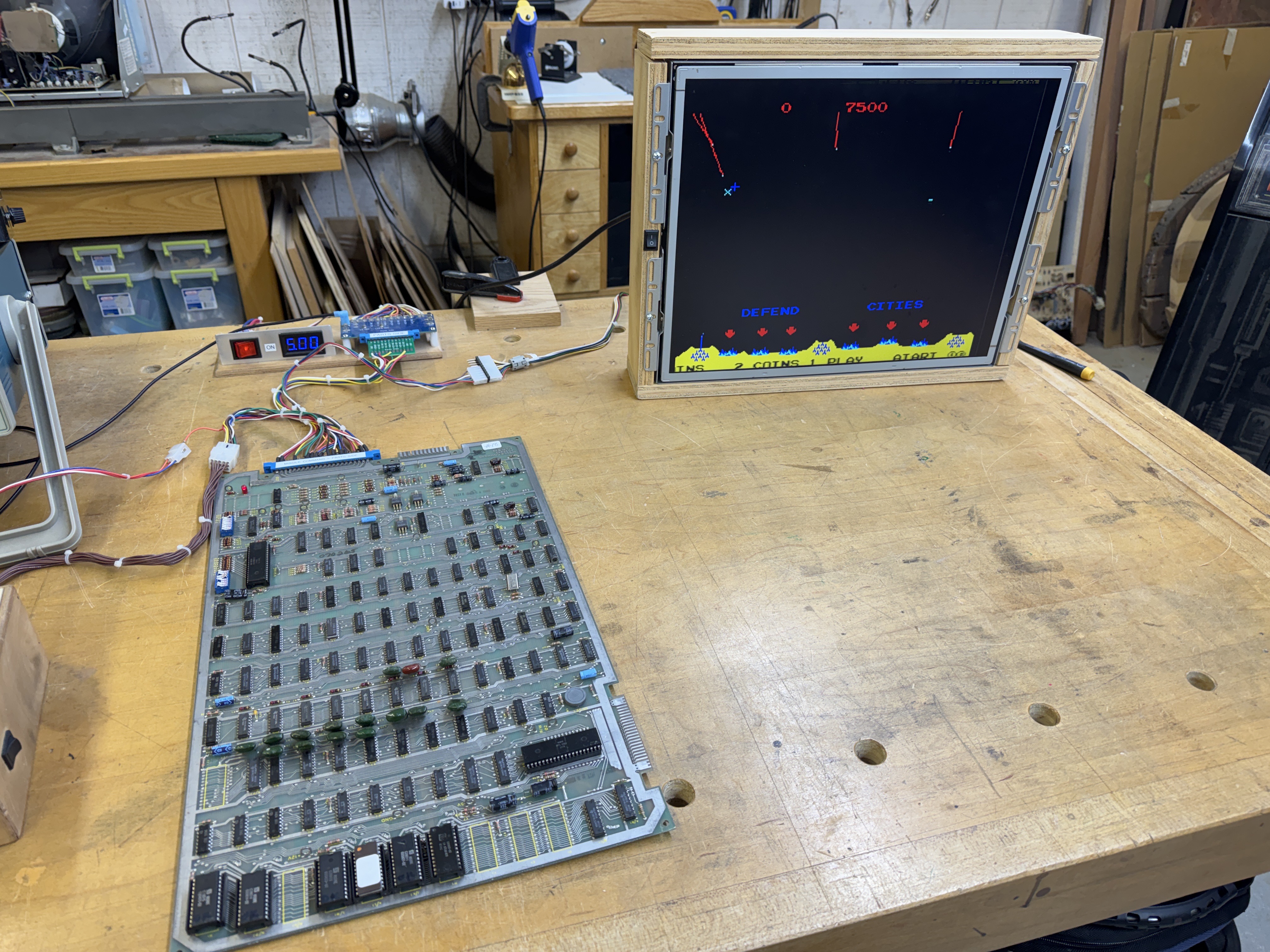
Board #17 – Board in for repair
Sent to me reported not working.. But it powered up for me. It does have a couple of issues that need to be addressed.

This finger repair works – but the spacing between them is too close. The edge connector has a bit too much play east-west and can short between pins if not placed perfectly. On the bench it dropped the voltage down to 2.8v (on my meter). I will replace these so that it can’t happen in the future. It may be why the board was reported not working..
Board has a Braze kit and these RAM replacements. Both work fine – I did remove the Braze for testing.
The issue it does have is this color bar static below the text crawl. It changes depending on the colors directly above it. That area should be black and off the screen. Missile Command has a funny sync signal and I have to reset my LCD to get it on the screen in the first place, notice the lettering off the top.
The finger edge was bothering me…


Removed the copper tape (which should have been soldered IMHO) and cleaned up the edges with Rust Erasers. They do the best job polishing up the metal. The second finger in was actually in good shape once I removed all of the goop from it.. Added fresh copper tape and used Liquid Tin to recoat all of the exposed copper.
The last part was finding the issue on the bottom. Missile Command has a strange setup on how it maps colors and treats the bottom 32 lines of the screen. This Website has some really good info. One new thing I learned is the Easter Egg diag modes (credit to the site above)
In self-test mode, there are some features not mentioned in the service manual:
- Slam + P1 left fire: draw full-screen grid
- Slam + P1 middle fire: draw color bars, erase screen, then exercise non-MADSEL read/write of video RAM
- Slam + P1 right fire: draw color bars

In diag – you can see the small vertical bars on the bottom and can cause them to rotate by hitting the fire buttons.. All that said – I spent a little too much time looking for the root cause..
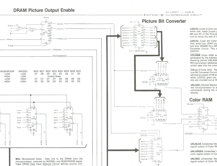
Probed all through this area trying to determine why I was getting color bits when they should have been off..

However – when I finally went backwards a bit I found the issue (and it makes sense…) 7404@E6 pin 4 was not reaching ground. /VBLANK was sorta 1/2 working.. Missile Command has a lot of VBLANKS..
Board works!
Board #18 – Board in for repair
Board sent in not working.
Initial testing showed that it had a bad EPROM. I compared to MAME.

The grey lines show where the issues work on the original ROM. I replaced it.
Here is a busted cap.. Likely wasn’t hurting anything, but it got replaced.
The CPU and Pokey Sockets were really loosely fitting. Both sockets got replaced.
Board works!
Board #19 – Board in for repair
This one was a quick fix when the owner was having trouble replacing a RAM.
Time was spent repairing the traces on the parts side (I don’t like solder side wire jumpers – they can snag and break). Parts side repairs get Kynar Wire trace fixes and I use UV Cured Resin to lock them in place before adding a socket.
Here are the jumpers locked in place with UV resin. This was right before the socket. I add extra flux here to get the solder to flow in the event the vias are damaged. It looks messier than it is..
The last RAM in the ROW was also bad.
Board works!
Board #20 – Board in for repair

Owner sent a couple of these in for repair. He purchased a few for a couple of cabinets that are being restored. This one seems to be a very early one. It has 2708 EPROMs which I don’t run into often.
I decided to connect to my tester first and check RAM/ROM.. Every other ROM tested and none of the RAM tested when I got started. I poked around a bit looking for a cause – but the board was really dirty and many times putting a ROM in would make one work and another would stop.. The board got washed. I use Krud Kutter to wash the boards. I use a finger brush on the back and a soft bristle paint brush on the front. I find the cleaner gets into the sockets and gets everything off the metal. The stuff is amazing and just melts the grime off.
Once it was cleaned up I cleaned all the socketed chip legs with a Rust Eraser and used Deoxit with a small paint brush and gave the contacts a coating.
The edge connector was poorly repaired at some point.


It was worse under the visible copper. I cut out the bad parts and cleaned it all up. A combination of fiberglass pen, UV Resin to fill the divot once cleaned out. The Rust Eraser block does a good job cleaning the edge and sanding the resin flat to the PCB. I use alcohol to clean between each step..


Last I add some copper tape and liquid tin to prevent the copper from oxidizing.
Now that I could get it all connected up and had clean chips. I connected the tester and sorted all of the EPROMs into their correct sockets. They verified correctly now that they were clean and in the right spot. RAM also verified too..
Put the CPU in.. not a lot going on..

Probing the CPU showed some activity.. but the sync pin (Pin 7) was dead.. Needs a 6502. Once that was in place.. Flashy screen..
I spent a little time looking for this issue.. The blinking is what threw me off.. In the end it was the color RAM@L7 that was bad.. While I was at it.. the can on the crystal was loose as many are on this game board. I replaced it with a low profile version. From here I let it run over night.. and the next day..
It failed.. I prefer they die in my shop.. so this is good.

The 74109@D6 failed Pin 9,10.. Replaced it. Owner also asked me to restrap the board for 2716’s so that it would be simpler to service and more reliable.
I test all the boards through 3 different cycles – After the 24 hour power cycle test – the board failed. Good – better here than in your machine!
Testing showed the VSYNC signal was missing.

Probing backwards through the sync circuit, VSYNC gets fed by VBLANK. The 74S260@A5 Pin 6 was dead.. I ran the board a couple extra days of testing. This one had sat on a shelf for years.
Board works!
Board #21 – Board in for repair
This one came in with Board#20. I was cleaning chips etc on that board, so I did this one at the same time.
First up –
@Y1 – no crystal.. Not going to do anything without that..
This board wasn’t as dirty as #20 – but I washed it because the ROMs also were quite “crunchy” going into and out of the sockets. After that on the tester I had 1 bad ROM (replaced it) added a label to one of the originals and replaced another because of a brittle leg that broke during cleaning.
Testing RAM and ROM with the FPGA Tester showed memory errors and other odd behavior.. I removed the Pokey and all the RAM and ROM passed now. The second time in a couple days where a Pokey was corrupting data on the bus.
Now that I have a replacement Pokey, good RAM and good ROM.. plugged in the CPU.. and nothing worked.. I swapped in a known good one and the game was trying to boot but was stuck. Disabling the watchdog and putting it into DIAG mode showed RAM good and ROM good. At least it was executing code!
Tracing through the watchdog circuit.

The usual suspects were not the cause (counter or gates near the reset line..) it was the actual /WDOG signal that should be coming out of the 7442@E8 – it wasn’t! Replacing it got the system and watchdog running normally.. It lasted about 15 minutes and then this..
Connecting to the tester.. The normal RAM memory test range is 0x0000 – 0x3FFF for Missile Command. After a bit of testing and adjusting.. I determined the RAM wasn’t being accessed correctly from 0x3000 – 0x3FFF. I spent a fair amount of time in the addressing part of the memory circuit.

I checked all through here and the supporting areas and it all had to be working because it worked for the lower address ranges.. I focused on DEAD6 because grounding it caused the screen noise to go away while I was testing. But not much was making sense.. Then I had an idea..
Test 0x2FFF and then test 0x3000.. Just the one byte and see what happens.. I already knew it was an addressing issue.. I just didn’t know what signal was missing.. Once I did that.. It was the /WPx on Pin3 of the RAM that had stopped.. finally.. something that made sense.
Backtracking though the addressing..

It appeared it was the 7432@J7 pin6 that was not firing properly.. I swapped it out – but no.. I should have went a bit further back..

To the 7442@N2.. Pins 1,2,3,4 are all used to decode /RAM addresses.. one of them was dead so the address range at 0x3000 -> was not being enabled.. I was looking on the more complex side of the addressing when it was really on the simple side right at the decoder chip..
Turns out.. Same date code as the 7442 I replaced above that was causing the watchdog to fail. During the first 12 hour test, the board stopped working after a couple hours (oddly).. Turned out it needed one of the ROMs cleaned a bit better. I ran this board a couple extra days too.
Board works!
Board #22 – Board in for repair
Owner sent this in with an ARII that they were having issues with. Wanted the board and ARII checked. The ARII DID have problems and I rebuilt that.. The Missile Command worked fine when I connected it all up.. It is for a machine in an arcade and I was asked to ‘look it over’.
For a board that worked.. It actually had a lot of problems.
As with all repairs, I removed all of the socketed chips, cleaned and Deoxit the legs & sockets and put it all back together. Ran it over night and it seemed fine. I always add a credit and if it is there 12+ hours later- that’s good. In hindsight.. can’t remember if I checked. My controller has a credit LED so that I can actually test the LED output and I can tell if there is a credit. I also ran my power cycle test and the board booted up as it is now.
Once I got to going down my checklist.. that’s when the little issues popped in.. I generally will flex and physically hit the board a little to see if it resets. It did.. Giving the ROMS a little twist revealed the last one in the row needed a socket and one of the others were touchy..
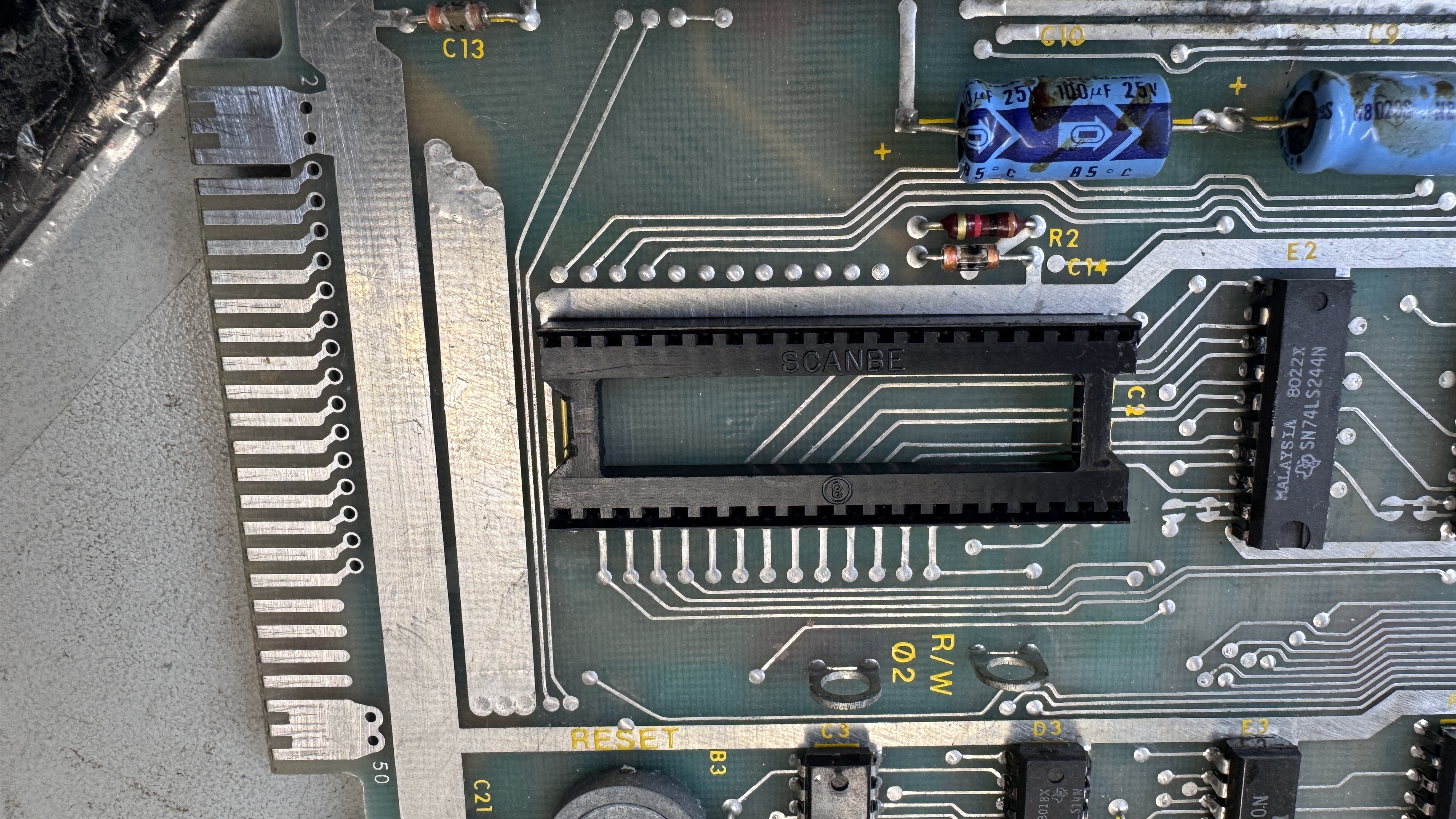
SCANBE sockets.. They are not always bad, but they are often bad. I ended up replacing all of the sockets on the board. I don’t remember seeing them on a Missile Commend before either, but they were factory. After that, no more reboots from physical board movement.. good! right?
Ran it over night again – no credit.. that’s not good.. Now I had the game up while working on another boardset on my other bench.. about 10 minutes later.. credit is gone.. another reset.. ugghhh.
I’ve had a rash of marginal Pokeys lately and swapped one in.. reset in about 10 min or so.. Well, at least it wasn’t that..
Then I looked closely at the CPU..
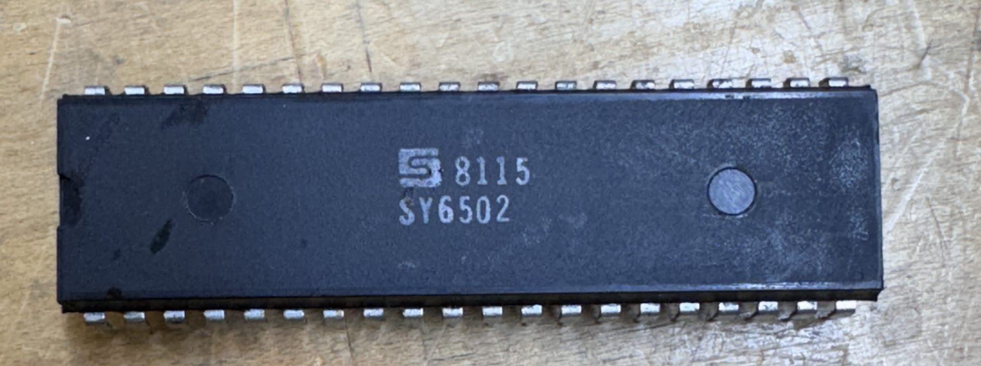
See the problem? ….. It needs a 6502A. 6502 technically cannot handle the higher clock speed. Replaced the CPU and it ran 18 hours without a reset..
While play testing.. It seemed like the volume was low.. All the sounds were there and sounded right, with the speaker pot all the way up.. not very loud..
Had a bad LM324. One of my more backwards repairs.
Board works!
Board #23 – Board in for repair
This one had a handful of issues. A few of the green gumdrop caps were missing and a few more were broken. The PCB also is an earlier revision that uses the 2708 EPROMs. But I had to start at the burned up edge connector.
Here are the stages of repair: cut off loose metal, clean and level the area if it burned up and got pitted. I use UV Cured resin for this. A little sanding makes it level with the board. The copper tape and some liquid tin to finish it off.
Connected to the board and no clock.
No crystal.. that will do it.. Put a new crystal in place.
From there – none of the ROM read correctly and I removed all of them. That cleared the busses and the RAM read correctly. One at a time I added the ROM and tested them. I have no way to burn 2708’s, but I had some left over from conversions and replaced 4 bad ROMs.
I replaced all 16 of the gumdrop caps with new much smaller caps. I will likely do this going forward on Missile Commands with the green caps which are fragile and often broken/missing.
During the burn in test cycle – something failed.
Switching to test mode – you can see and hear something is broken. The strange part is the game worked, all the buttons worked, the trackball was very laggy going to the left. Using the FPGA Tester I determined the machine was having difficulty reading the SLAM switch (it seemed). I could not manually trigger it. After looking at all the glass ceramic caps looking for a short I pulled the 74LS245@M9 and replaced it. That corrected the slam issue – but I was still having the issue in the video above. Pulling pin1 high on 74LS245@L9 stopped all of the beeping. The tester showed that Fire Right 2 (for cocktail players) also read stuck. Replacing L9 fixed that.
Both failed the same way.. @M9 and @L9 Replacing them also fixed the laggy trackball issue.
Board works!
Board #24 – Board in for repair
This one came through stripped.. It clearly came from a stash. No CPU, no EPROMS. It was missing the 74LS175@#L8. Before I did anything I tested the Pokey – which worked. Otherwise this one may not have been worth the repair expense. But it worked.
The edge connector had been sanded/cleaned a number of times. I had to clean it again – but some copper was coming through. It got retinned.
It was also pretty nasty.. So into the sink. Krud Kutter is by far the best cleaner for these. Spray a lot on with the board dry. Wait 5 minutes and brush with a soft bristles. Rinse and I dry using compressed air. I find that Krud Kutter cleans the contacts in the sockets better than you would expect.
Once connected to the tester – clock was messed up. Another bad crystal. Next, RAM@F4 was bad. I replaced it.
Burned a full set of 6 EPROMs and added a 6502A. In the above pics, I had already replaced all of the green gumdrop caps. It was ready to go with the board before it.
Board works!

bonjour,
Je recherche quelqu’un pour me réparer une pcb Atari missil command.
Merci pour votre retour.
Cordialement